Stacked gate semiconductor memory and manufacturing method for the same

a manufacturing method and semiconductor technology, applied in semiconductor devices, transistors, instruments, etc., can solve the problems of non-uniform distortion of the geometries and sizes of the respective memory cells, and the difficulty of achieving highly integrated stacked gate memory cells with reduced power dissipation

Inactive Publication Date: 2005-08-25
KK TOSHIBA
View PDF2 Cites 57 Cited by
  • Summary
  • Abstract
  • Description
  • Claims
  • Application Information

AI Technical Summary

Benefits of technology

[0014] An aspect of the present invention inheres in a semiconductor memory embracing a plurality of memory cell transistors, each of the memory cell transistors encompassing (a) a substrate; (b) a gate insulator stacked on the substrate, configured to enable tunneling of electrons through the gate insulator; (c) a floating gate electrode stacked on the gate insulator, configured to accumulate electron charges; (d) an inter-electrode dielectric stacked on the floating gate electrode incorporating a positive charge layer, distribution of the positive charge layer being localized in the lower half of the inter-electrode dielectric; and (e) a control gate electrode stacked on the inter-electrode dielectric.

Problems solved by technology

However, the miniaturization of memory cells causes problems of non-uniform distortion of the geometries and sizes of the respective memory cells due to processing unevenness, pattern misalignments caused during lithography processes, or the like.
As described above, since high program and erase gate voltages are needed for the earlier stacked gate memory cells, achievement of highly integrated stacked gate memory cells with reduced power dissipation is difficult.

Method used


Image

  • Stacked gate semiconductor memory and manufacturing method for the same
  • Stacked gate semiconductor memory and manufacturing method for the same
  • Stacked gate semiconductor memory and manufacturing method for the same

Examples


first embodiment

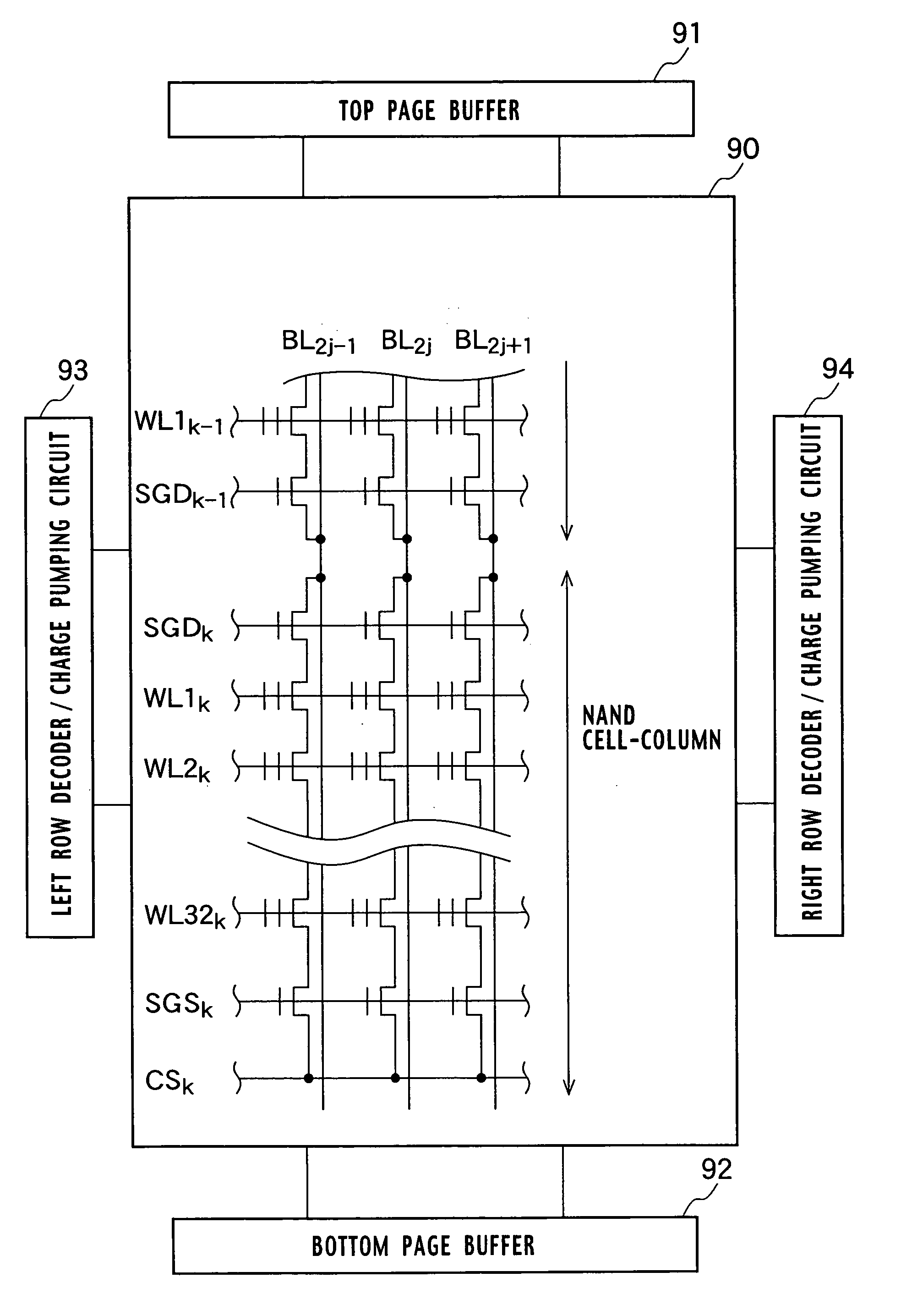
[0076]FIG. 4 is a block diagram illustrating a schematic circuitry of NAND flash memory as a semiconductor memory according to a first embodiment of the present invention. Peripheral circuits (91, 92, 93, and 94) such as a top page buffer 91, a bottom page buffer 92, a left row decoder / charge pump 93, and a right row decoder / charge pump 94 are arranged on the periphery of a memory cell matrix 90.

[0077] As shown in FIGS. 4 and 5, the memory cell matrix 90 embraces plural cell columns (NAND cell columns) extending along a column-direction, the cell columns are arranged along a row-direction in parallel. Each of the cell columns is implemented by plural memory cell transistors serially arranged along the column-direction. Each of the memory cell transistors has a charge accumulation layer whose electric charge accumulation level is configured to be controlled separately. The horizontal lines connected to all the memory cell transistors in corresponding rows are called “the word lines ...

second embodiment

[0124] Similar to the semiconductor memory according to the first embodiment, a second embodiment of the present invention has a memory cell matrix, which embraces plural cell columns (NAND cell columns) extending along a column-direction, the cell columns are arranged along a row-direction in parallel. Plural memory cell transistors serially arranged along the column-direction implement each of the NAND cell columns. Each of the memory cell transistors is implemented by a stacked gate architecture, in which a charge accumulation layer is encompassed. Each of the electric charge accumulation levels in the respective charge accumulation layers, which are arranged in a matrix form, is controlled separately. FIG. 22 is a cross sectional view showing a corresponding part of the memory cell matrix 90 taken on line VB-VB in FIG. 5.

[0125] As shown in FIG. 22, the memory cell matrix of the semiconductor memory according to the second embodiment encompasses: device isolation films 7, which ...

third embodiment

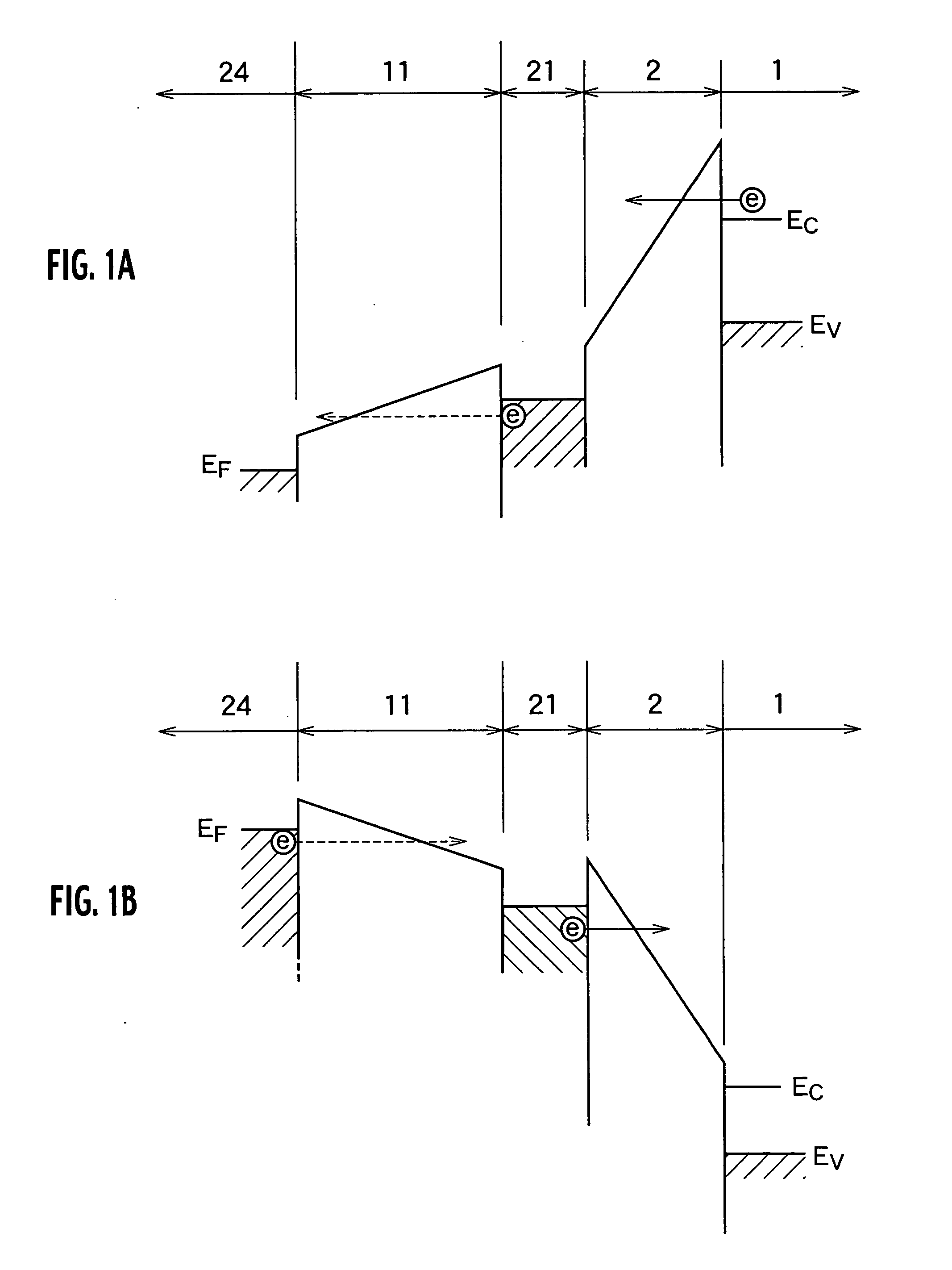
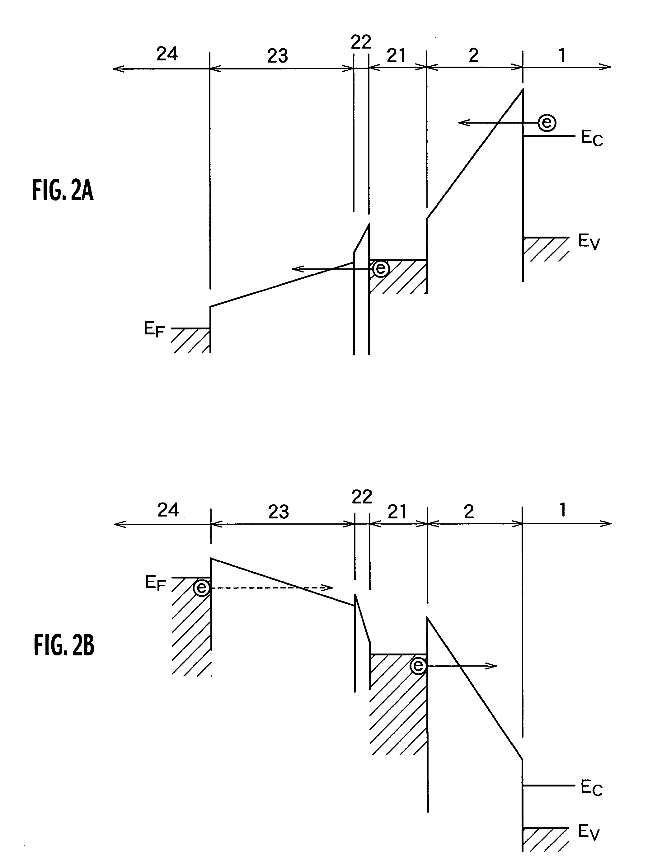
[0156] As shown in FIG. 7B, in the erase operation of the semiconductor memory according to the first embodiment, when the erase gate voltage applied to the control gate electrode 24, which is determined so that a desired tunneling current can flow through the gate insulator 2, increases higher than the voltage in the case where there is no positive charge layer, since the effective tunneling distance established in the inter-electrode dielectric 11 becomes shorter, the amount of tunneling leakage current flowing through the inter-electrode dielectric 11 increases. A more preferable structure for suppressing such tunneling leakage current will be explained, referencing energy band diagrams shown in FIGS. 34A and 34B, in a semiconductor memory according to a third embodiment.

[0157] Similar to the structure shown in FIGS. 6A and 6B, in the semiconductor memory according to the third embodiment, each of the memory cell transistors is implemented by a stacked gate architecture, in whic...


PUM


Abstract

A semiconductor memory embraces a plurality of memory cell transistors, and each of the memory cell transistors encompasses a substrate; a gate insulator stacked on the substrate, configured to enable tunneling of electrons through the gate insulator; a floating gate electrode stacked on the gate insulator, configured to accumulate electron charges; an inter-electrode dielectric stacked on the floating gate electrode incorporating a positive charge layer, distribution of the positive charge layer being localized in the lower half of the inter-electrode dielectric; and a control gate electrode stacked on the inter-electrode dielectric.

Description

CROSS REFERENCE TO RELATED APPLICATIONS [0001] This application claims benefit of priority under 35 USC 119 based on Japanese Patent Application No. P2004-042622 filed Feb. 19, 2004, the entire contents of which are incorporated by reference herein. BACKGROUND OF THE INVENTION [0002] 1. Field of the Invention [0003] The present invention relates to a semiconductor memory and a fabrication method for the semiconductor memory. In particular, it relates to gate structures of memory cells for the semiconductor memories in which miniaturization of cell size has advanced. [0004] 2. Description of the Related Art [0005] In accordance with the advancement of semiconductor technology, especially with the development of microelectronic fabrication technology, miniaturization of memory cells and high integration of semiconductor memories have progressed. However, the miniaturization of memory cells causes problems of non-uniform distortion of the geometries and sizes of the respective memory c...

Claims


Application Information

Patent Timeline
Patent Type & Authority Applications(United States)
IPC IPC(8): G11C16/04H01L21/8247H01L27/115H01L29/788H01L29/792H01L29/94
CPCG11C16/0416G11C16/0483H01L27/115H01L27/11529H01L27/11524H01L27/11526H01L27/11521H10B69/00H10B41/41H10B41/35H10B41/30H10B41/40
Inventor OZAWA, YOSHIO
Owner KK TOSHIBA
Why Eureka
Try Eureka