Semiconductor device

a technology of semiconductor devices and semiconductors, applied in the direction of semiconductor devices, connection to earth, contact member materials, etc., can solve the problems of insufficient expansion of depletion layer b>50/b>, inability to secure predetermined breakdown voltages, and inability to reduce forward voltage vf. progress

Inactive Publication Date: 2005-08-25
SANYO ELECTRIC CO LTD
View PDF15 Cites 10 Cited by
  • Summary
  • Abstract
  • Description
  • Claims
  • Application Information

AI Technical Summary

Problems solved by technology

Therefore, there is a problem in that the extension of the depletion layer 50 is insufficient and the predetermined breakdown voltage can not be secured.
Thus, there is a problem in that, when a current path is narrowed by providing the p+ type region 33, a reduction in the forward voltage VF does not make progress.
However, it is extremely difficult to perform control for obtaining a predetermined forward voltage VF characteristic and the leak current IR characteristic and, then, securing a predetermined breakdown voltage.

Method used


Image

  • Semiconductor device
  • Semiconductor device
  • Semiconductor device

Examples


Embodiment Construction

[0023] An embodiment of the invention will be explained in detail with reference to FIGS. 1A and 1B to FIGS. 3A and 3B.

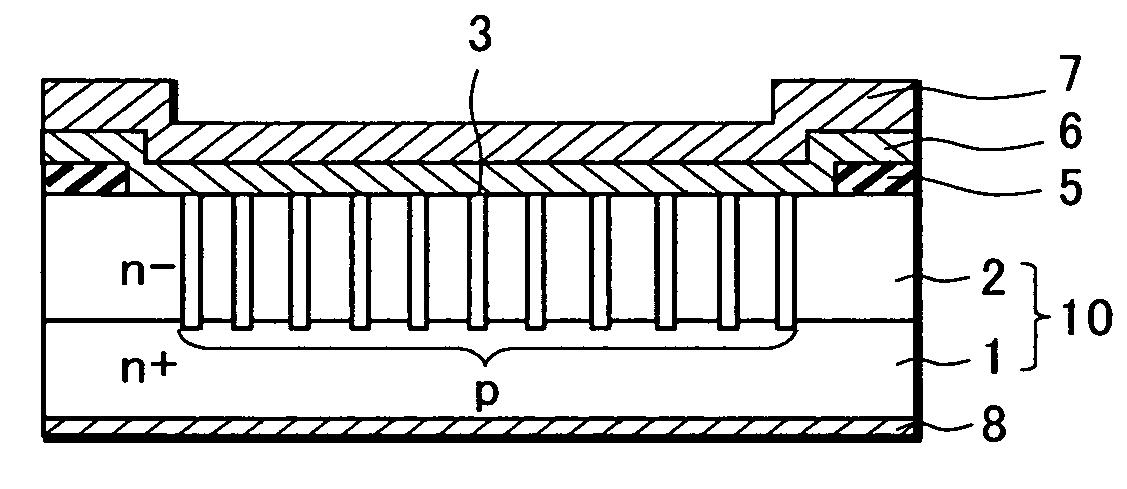
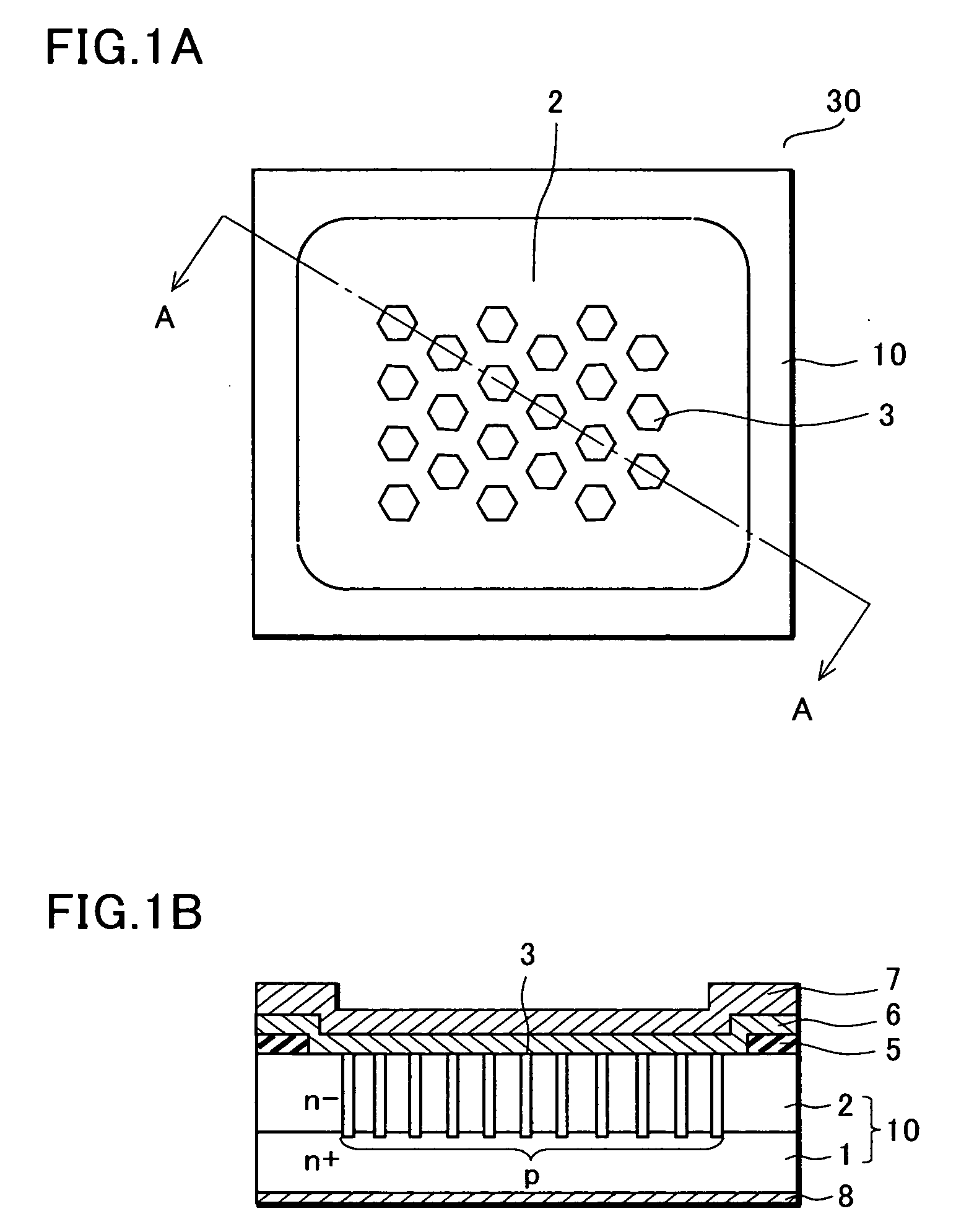
[0024]FIGS. 1A and 1B show a Schottky barrier diode according to the embodiment of the invention. FIG. 1A is a plan view of the Schottky barrier diode and FIG. 1B is a sectional view along line A-A in FIG. 1A. Note that a Schottky metal layer and an anode electrode on a surface of a substrate are not shown in FIG. 1A.

[0025] The Schottky barrier diode of the embodiment includes a one conduction type semiconductor substrate 1, a one conduction type semiconductor layer 2, reverse conduction type semiconductor regions 3, and a Schottky metal layer 6.

[0026] A substrate 10 is obtained by stacking the n− type semiconductor layer 2 on the n+ type silicon semiconductor substrate 1 according to, for example, an epitaxial growth method.

[0027] The reverse conduction type semiconductor regions 3 are p type semiconductor regions provided in the n− type semiconductor layer 2. F...


PUM


Abstract

Conventionally, VF and IR characteristics of a Schottky barrier diode are in a tradeoff relation and there is a problem in that an increase in a leak current is unavoidable in order to realize a reduction in VF. To solve the problem, p type semiconductor regions of a pillar shape reaching an n+ type semiconductor substrate are provided in an n− type semiconductor layer. When a reverse voltage is applied, a depletion layer expanding in a substrate horizontal direction from the p type semiconductor regions fills the n− type semiconductor layer. Thus, it is possible to prevent the leak current generated on a Schottky junction interface from leaking to a cathode side. Since an impurity concentration of the n− type semiconductor layer can be increased to a degree at which the depletion layer expanding from the p type semiconductor regions adjacent to each other can be pinched off, it is possible to realize a reduction in VF and it is possible to secure a predetermined breakdown voltage if only the depletion layer is pinched off.

Description

BACKGROUND OF THE INVENTION [0001] 1. Field of the Invention [0002] The present invention relates to a semiconductor device, and in particular to a semiconductor device that realizes a reduction in a forward voltage VF and a reduction in a reverse current IR of a Schottky barrier diode and secures a predetermined breakdown voltage. [0003] 2. Description of the Related Art [0004] A Schottky junction formed by a silicon semiconductor substrate and a metal layer has a rectification action because of a barrier thereof. Thus, the Schottky junction is an element that is generally well known as a Schottky barrier diode. [0005]FIGS. 4A and 4B show a conventional Schottky barrier diode. [0006] As shown in FIG. 4A, an n− type semiconductor layer 32 is stacked on an n+ type semiconductor substrate 31, and a Schottky metal layer 36, which forms a Schottky junction with a surface of the n− type semiconductor layer 32, is provided. This metal layer is made of, for example, Ti. Moreover, an Al lay...

Claims


Application Information

Patent Timeline
Patent Type & Authority Applications(United States)
IPC IPC(8): H01L29/872H01L29/47H01L29/861H01L31/062
CPCH01L29/872H01L29/861H01R4/66H02G13/40
Inventor OKADA, TETSUYASAITO, HIROAKI
Owner SANYO ELECTRIC CO LTD
Why Eureka
Try Eureka