Organic electroluminescent device

a technology of electroluminescent devices and organic el, which is applied in the direction of discharge tubes, luminescent screens, instruments, etc., to achieve the effects of improving brightness lifetime, effective energy gap, and improving brightness lifetim

Inactive Publication Date: 2005-08-25
DENSO CORP
View PDF5 Cites 55 Cited by
  • Summary
  • Abstract
  • Description
  • Claims
  • Application Information

AI Technical Summary

Benefits of technology

[0030] Since a tertiary amine compound having an ionization potential different from that of the electron transporting material by 0.35 eV or greater and constituting the hole transporting material has only one oxidation potential as determined by the cyclic voltammetry, which fact has been found by experiment, use of it makes it possible to secur

Problems solved by technology

As the oxidation potential of the tertiary amine compound, that is, the hole transporting material is higher, the transfer of holes from the hole transporting materia

Method used


Image

  • Organic electroluminescent device
  • Organic electroluminescent device
  • Organic electroluminescent device

Examples


investigation example 1-1

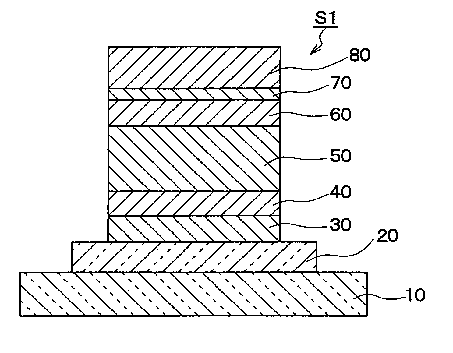
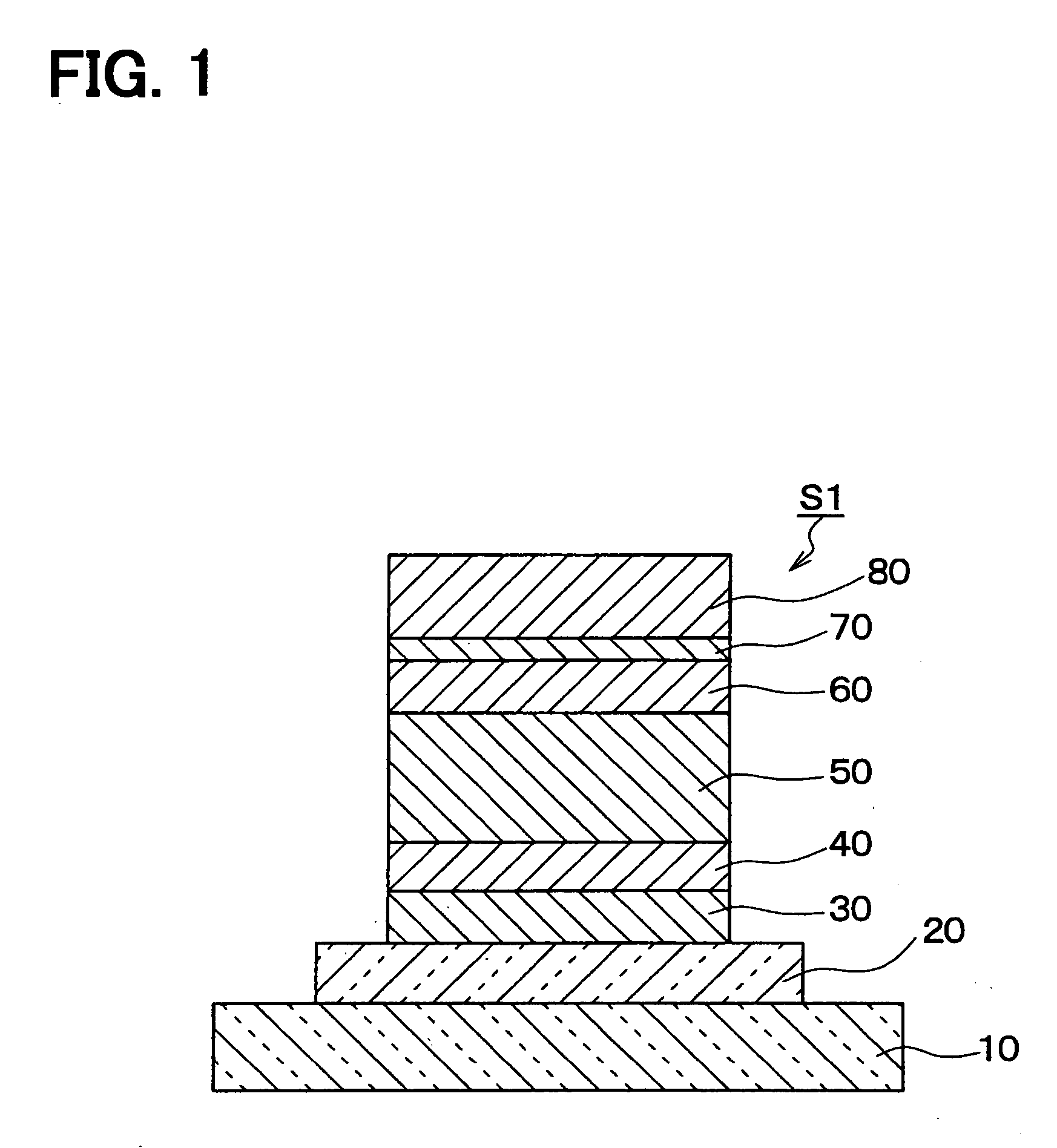
[0100] Over a glass substrate 10, an ITO film (clear electrode) was formed as an anode 20. The surface of the substrate was adjusted to Ra of about 1 nm and Rz of about 10 nm by polishing.

[0101] Over the anode 20, a 10-nm hole injection layer 30 made of CuPc as an organic material having crystallinity was formed. Over the hole injection layer 30, a hole transporting layer 40 of 20 nm thick was formed using Compound 1, a tertiary amine compound.

[0102] Over the hole transporting layer 40, a light emitter layer 50 of 20 nm thick was formed using a 60:20:3 (weight ratio) mixture of Compound 1 as a tertiary amine compound, Compound 6 as an electron transporting material and Compound 8 as a light emitting additive.

[0103] An organic EL device was fabricated by successively forming, over the light emitter layer 50, Compound 6 of 20 nm thick as an electron transporting layer 60, tris(8-quinolinolato)aluminum of 10 nm thick, LiF as an electron injection layer 70, and Al as a cathode 80 and...

investigation example 1-2

[0105] By using a similar device structure under similar device fabricating conditions to Investigation Example 1-1 except for the use of Compound 7 as the electron transporting material used for the light emitter layer 50 and the layer of the electron transporting layer 60 on the side of the light emitter layer 50, a device was fabricated.

[0106] Durability test of the resulting device was carried out under the circumstance of 85° C., initial brightness of 400 cd / m2 and 1 / 64 duty driving. The results are as shown in Table 1. The remarkable appearance of spots was not observed even when the storage test under the circumstance of 100° C. was conducted for 500 hours or greater.

investigation example 2-1

[0107] By using a similar device structure under similar device fabricating conditions to Investigation Example 1-1 except for the use of Compound 2 as the tertiary amine compound used for the hole transporting layer 40 and light emitter layer 50, a device was fabricated.

[0108] Durability test of the resulting device was carried out under the circumstance of 85° C., initial brightness of 400 cd / m2 and 1 / 64 duty driving. The results are as shown in Table 1. The remarkable appearance of dark spots was not observed even when the storage test under the circumstance of 100° C. was conducted for 500 hours or greater.


PUM

PropertyMeasurementUnit
Glass transition temperatureaaaaaaaaaa
Ionization potentialaaaaaaaaaa
Massaaaaaaaaaa

Abstract

An organic EL device includes a pair of electrodes, a light emitter layer obtained by mixing a hole transporting material made of a tertiary amine compound, an electron transporting material and a light emitting additive. The tertiary amine compound constituting the hole transporting material has only one oxidation potential as measured by the cyclic voltammetry. A difference in ionization potential between the hole transporting material and electron transporting material of the light emitter layer is 0.35 eV or greater.

Description

CROSS REFERENCE TO RELATED APPLICATIONS [0001] This application is based upon, claims the benefit of priority of, and incorporates by reference the contents of, Japanese Patent Application No. 2004-49462 filed on Feb. 25, 2004 and Japanese Patent Application No. 2004-302986 filed on Oct. 18, 2004. FIELD OF THE INVENTION [0002] The present invention relates to an organic EL (electroluminescent) device, and, more particularly, to such a device using, as a host of its light emitter layer, a mixed host of a hole transporting material and an electron transporting material. BACKGROUND OF THE INVENTION [0003] As being self-luminescent, organic EL devices have excellent visibility. They can be driven at a voltage as low as several volts to tens of volts so that the weight of the device including a driving circuit can be reduced. Such characteristics make it possible to use them as a thin film display, illumination and back light. Rich color variation is also one characteristic of organic EL...

Claims


Application Information

Patent Timeline
IPC IPC(8): C09K11/06H01L51/50H01J1/62H01L51/00H01L51/52H05B33/14
CPCH01L51/0058H01L51/0059H01L2251/308H01L51/5012H01L51/5206H01L51/0081Y10S428/917H10K85/631H10K85/626H10K85/324H10K50/11H10K50/81H10K2101/30H10K2102/103G01B7/02
Inventor KATO, TETSUYAKOJIMA, KAZUSHIGE
Owner DENSO CORP
Why Eureka
Try Eureka