Microcontact printing method using imprinted nanostructure and nanostructure thereof

a nanostructure and printing method technology, applied in the direction of bridge structure details, bridge erection/assembly, chemical vapor deposition coating, etc., can solve the problem of elastomer material sagging, inaccurate record cannot be made due to flexible pims, and it is difficult to have an independent processing condition

Inactive Publication Date: 2005-08-25
KOREA INST OF MACHINERY & MATERIALS
View PDF6 Cites 59 Cited by
  • Summary
  • Abstract
  • Description
  • Claims
  • Application Information

AI Technical Summary

Problems solved by technology

However, With the microcontact printing process, it is difficult to have an independent processing condition due to several problems in processing.
In the current patterning molding process, problems include: a paring problem in that gravity, adhesive strength, and capillary forces are exerted on the elastomer material to collapse a shape thereof or incur defects; a sagging problem in that the elastomer material sags when a ratio of a patterned portion to the remaining non-patterned portion is low; and a shrinking problem in that an accurate record cannot be made due to a flexible PIMS.
However, the microcontact printing process does not yet meet the requirement of a fine line pattern for a complicated electronic apparatus.
The conventional microcontact printing process can implement a micro pattern of up to 300 nm due to the characteristics of polymer, while it is almost impossible to implement the micro pattern of less than 100 nm due to poor resolution and excessive defects.
In addition, when fabricated in a multi-layered structure, the conventional microcontact printing process has a problem in that misalignment may occur due to deformation of the pattern and distortion of the structure during a deposition process.

Method used


Image

  • Microcontact printing method using imprinted nanostructure and nanostructure thereof
  • Microcontact printing method using imprinted nanostructure and nanostructure thereof
  • Microcontact printing method using imprinted nanostructure and nanostructure thereof

Examples


Embodiment Construction

[0029] Now, an exemplary embodiment of the present invention will be described with reference to the attached drawings so that those skilled in the art can easily practice the present invention.

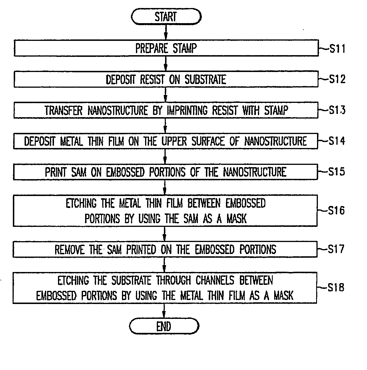
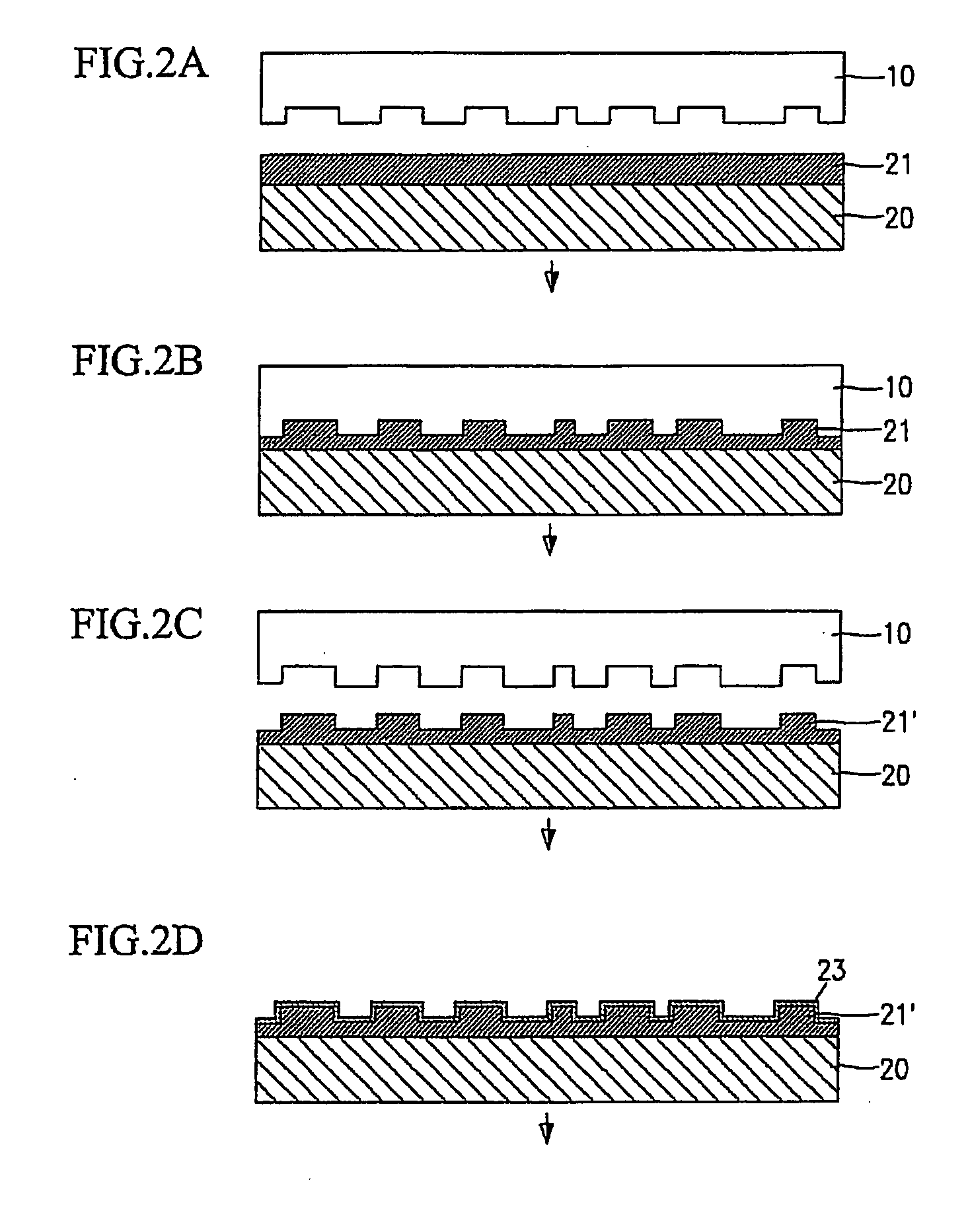
[0030]FIG. 1 is a flow chart for explaining a microcontact printing method using a nanoimprint lithography process according to an exemplary embodiment of the present invention, and FIG. 2A through 2I are diagrams for explaining steps thereof.

[0031] As shown in FIG. 1, in the complex microcontact printing method according to the present invention, a substrate 20 on which a nanostructure is transferred from a stamp 10 is prepared. Next, the substrate 20 is patterned with the microcontact printing method.

[0032] Therefore, the process according to an embodiment of the present invention starts with a step of preparing a stamp 10 (S11). The stamp 10 has a pattern corresponding to a nanostructure to be formed. With a UV nanoimprint lithography process, it is desirable that the stamp 10 be made o...


PUM

PropertyMeasurementUnit
wavelengthaaaaaaaaaa
depthaaaaaaaaaa
depthaaaaaaaaaa

Abstract

A microcontact printing method using an imprinted nanostructure is provided, wherein the microcontact printing is introduced to a nanoimprint lithography process to pattern a self-assembled monolayer (SAM) The method includes forming a nanostructure on a substrate by using the nanoimprint lithography process; and patterning the nanostructure with the microcontact printing method. The operation of patterning includes: depositing a metal thin film on the nanostructure; contacting a plate with the nanostructure to selectively print the SAM on the nanostructure, wherein the SAM is inked on the plate and the metal thin film is deposited on the nanostructure; selectively removing the metal thin film by using the SAM as a mask; removing the SAM from the nanostructure; and patterning the substrate by using the remaining metal thin film on the nanostructure as a mask.

Description

CROSS REFERENCE TO RELATED APPLICATION [0001] This application claims priority to and the benefit of Korean Patent Application No. 10-2004-0012192, filed on Feb. 24, 2004, which is hereby incorporated by reference for all purposes as if fully set forth herein. BACKGROUND OF THE INVENTION [0002] (a) Field of the Invention [0003] The present invention relates to a microcontact printing method, and more specifically, to a microcontact printing method using a nanoimprinted nanostructure to transfer a pattern with a size of several tens of nanometers. [0004] (b) Description of Related Art [0005] Nanoimprint lithography technology is a technology for pressing a surface of a polymer resist coated on a substrate with a stamp having an imprinted nanostructure thereon to transfer the nanostructure. [0006] In the nanoimprint process initially developed by Prof. Chou at Princeton Univ. in 1996, a base sheet coated with a polymethylmethacrylate (PMMA) resist is pressed with a stamp having a nano...

Claims


Application Information

Patent Timeline
Patent Type & Authority Applications(United States)
IPC IPC(8): G03F7/00B05D1/36B32B3/00B81C1/00G03F1/00
CPCB81C1/0046B82Y10/00Y10T428/24917B82Y40/00G03F1/0007B82Y30/00E01D21/00E01D19/02
Inventor JEONG, JUN-HOSOHN, HYONKEESIM, YOUNG-SUKSHIN, YOUNG-JAELEE, EUNG-SUGWHANG, KYUNG-HYUN
Owner KOREA INST OF MACHINERY & MATERIALS
Why Eureka
Try Eureka