Methods of fabricating interconnects for semiconductor components

Active Publication Date: 2005-08-25
MICRON TECH INC
View PDF16 Cites 10 Cited by
  • Summary
  • Abstract
  • Description
  • Claims
  • Application Information

AI Technical Summary

Benefits of technology

[0013] In one aspect, the invention encompasses a method of fabricating an interconnect for a semiconductor component. A semiconductor substrate is provided, and an opening is formed which extends entirely through

Problems solved by technology

A problem is encountered in uniformly filling hole 130 with solder.
Specifically, the small dimension of hole 130

Method used


Image

  • Methods of fabricating interconnects for semiconductor components
  • Methods of fabricating interconnects for semiconductor components
  • Methods of fabricating interconnects for semiconductor components

Examples


Embodiment Construction

[0033] This disclosure of the invention is submitted in furtherance of the constitutional purposes of the U.S. Patent Laws “to promote the progress of science and useful arts” (Article 1, Section 8).

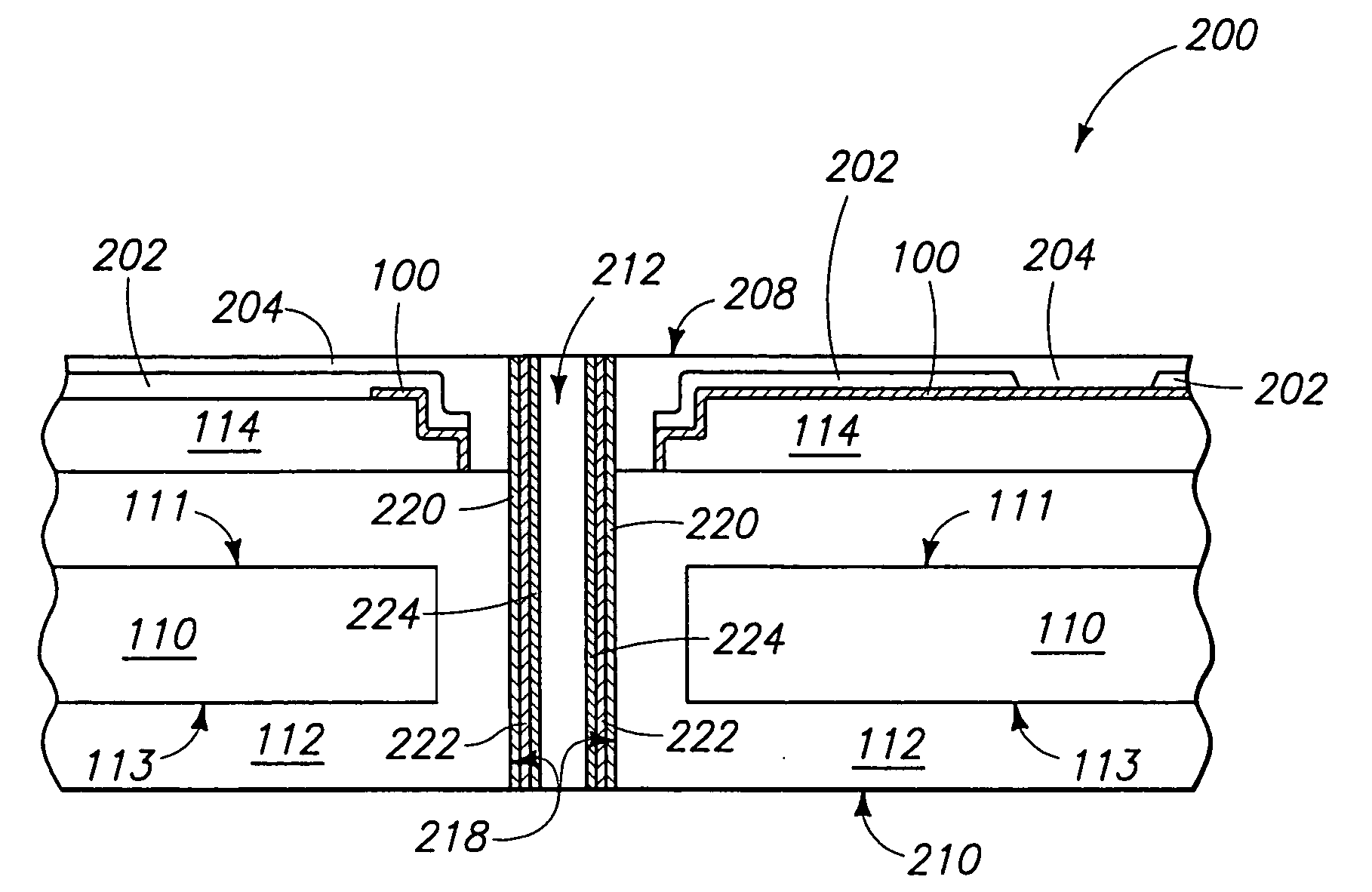
[0034] In particular aspects, the invention encompasses methods for forming solder within openings extending through semiconductor components. Low temperature deposition is utilized to form a film within an opening. The film can comprise a metal nitride, such as, for example, titanium nitride. A surface of the film is plated with a solder-wetting material (such as, for example, nickel). The plating can comprise activation of the surface, (such as, for example, by dipping the film in a solution comprising hafnium and / or palladium), followed by electroless plating of the activated surface with the solder-wetting material. Alternatively, the plating can comprise utilization of activationless plating chemistry to form a plating on the surface. The activationless plating chemistry can utiliz...


PUM

PropertyMeasurementUnit
Temperatureaaaaaaaaaa
Timeaaaaaaaaaa
Electrical conductoraaaaaaaaaa

Abstract

In one aspect, the invention encompasses a method of fabricating an interconnect for a semiconductor component. A semiconductor substrate is provided, and an opening is formed which extends entirely through the substrate. A first material is deposited along sidewalls of the opening at a temperature of less than or equal to about 200° C. The deposition can comprise one or both of atomic layer deposition and chemical vapor deposition, and the first material can comprise a metal nitride. A solder-wetting material is formed over a surface of the first material. The solder-wetting material can comprise, for example, nickel. Subsequently, solder is provided within the opening and over the solder-wetting material.

Description

TECHNICAL FIELD [0001] The invention pertains to methods of fabricating interconnects for semiconductor components. BACKGROUND OF THE INVENTION [0002] Semiconductor components, such as dice, wafers and chip scale packages, are fabricated to include external contacts to allow electrical connections to be made from the outside of the components to integrated circuits contained on the components. A semiconductor die, for example, typically includes patterns of bond pads formed on a face of the die. At the wafer level, the bond pads are used for probe testing the integrated circuits on the die. At the die level, the bond pads are used for testing, and also for making electrical connections, such as wire bonds, for packaging. Typically, the bond pads comprise planar aluminum pads, or alternatively solder bumps on solder wettable pads. [0003] The interconnects described above are but one type of interconnect that can be utilized with semiconductor components. Numerous other types of inter...

Claims


Application Information

Patent Timeline
IPC IPC(8): H01L21/768H01L23/48
CPCC23C16/34H01L2224/0401H01L21/28562H01L21/288H01L21/76898H01L23/481H01L24/11H01L24/13H01L2224/0231H01L2224/13009H01L2224/13099H01L2924/01013H01L2924/01022H01L2924/01029H01L2924/01033H01L2924/01046H01L2924/01047H01L2924/01073H01L2924/01078H01L2924/01082H01L2924/04941H01L2924/14H01L2924/01005H01L2924/01006H01L2924/01023H01L2924/01072H01L2924/01074H01L2924/014C23C18/1879C23C18/1608C23C18/36H01L2224/13111C23C16/45525H01L2224/13024H01L2224/02372H01L2924/0001H01L2924/00014H01L2224/03002H01L2924/12042H01L2924/00H01L21/70H01L23/48H01L21/768
Inventor KIRBY, KYLE K.MENG, SHUANGDERDERIAN, GARO J.
Owner MICRON TECH INC
Why Eureka
Try Eureka