
Organic light-emitting device and method of fabricating the same

a light-emitting device and organic technology, applied in the direction of thermoelectric devices, electroluminescent light sources, electric lighting sources, etc., can solve the problems of deteriorating display performance and large light-emitting area than predetermined, and achieve the effect of improving display performance, reducing manufacturing costs, and improving light leakage in non-pixel areas

Inactive Publication Date: 2005-09-01
INNOLUX CORP
View PDF4 Cites 57 Cited by
  • Summary
  • Abstract
  • Description
  • Claims
  • Application Information

AI Technical Summary

Benefits of technology

[0008] The present invention provides an organic light-emitting device and method of fabricating the same to ameliorate light leakage in non-pixel areas and improve display performance without significantly complicating the fabrication process or increasing the number of lithography steps.

Problems solved by technology

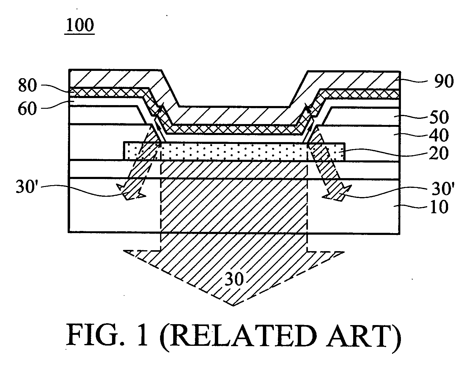
Because the silicon oxide pattern 40 is pervious to light, the emitted light 30′ thereby penetrates through the silicon oxide pattern 40 and the transparent substrate 10, resulting in light-leakage and a larger light-emitting area than predetermined, deteriorating display performance.

Method used


Image

  • Organic light-emitting device and method of fabricating the same
  • Organic light-emitting device and method of fabricating the same
  • Organic light-emitting device and method of fabricating the same

Examples


Embodiment Construction

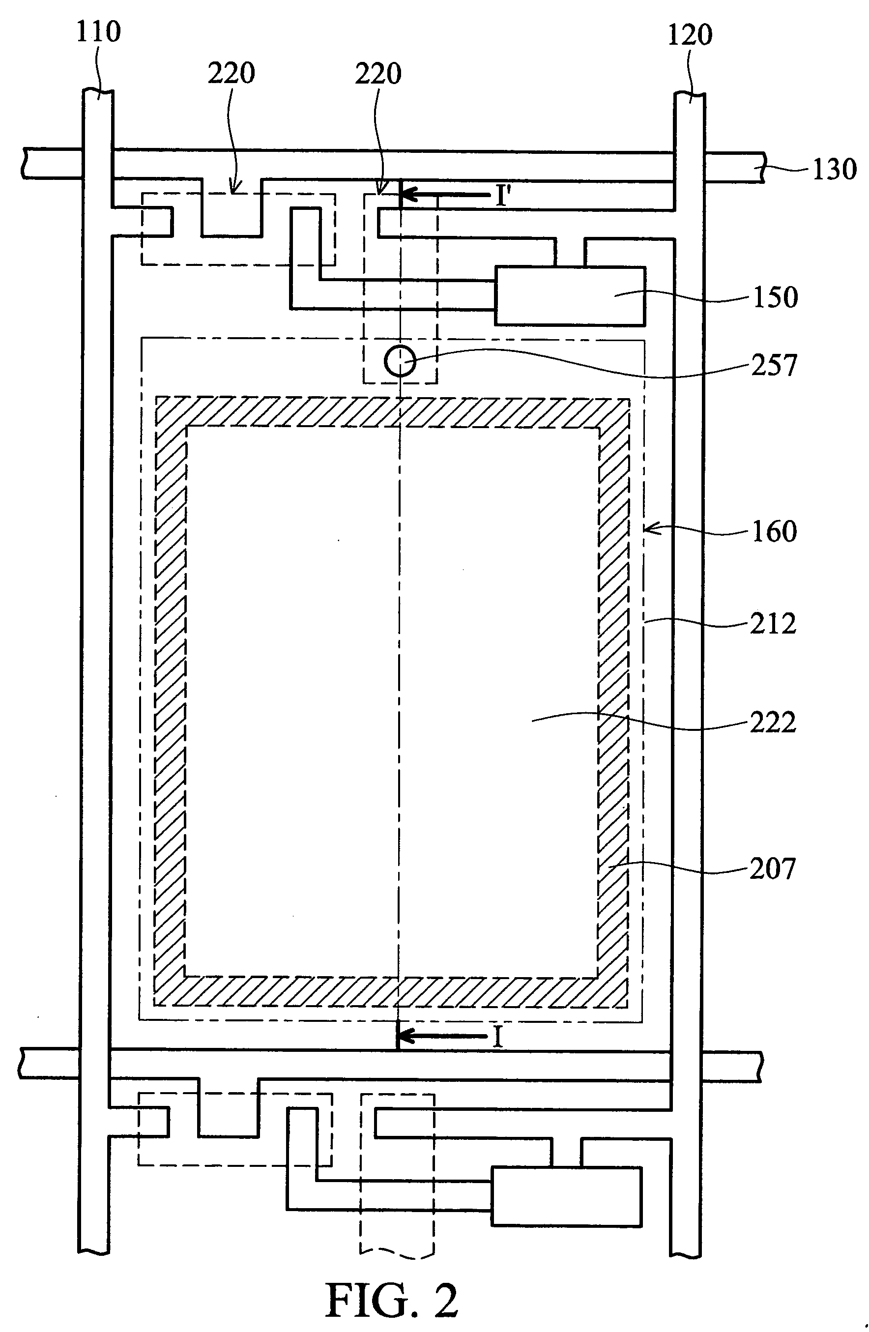
[0018]FIG. 2 is a schematic plan view illustrating an OLED device of active matrix drive type according to an embodiment of the present invention.

[0019] The driving matrix of the present invention may be an a-Si (amorphous silicon) TFTs array or an LTPS (low temperature polysilicon) TFTs array disposed on a transparent substrate of, for example, glass substrate.

[0020] In one embodiment, a driving matrix substrate of an LTPS array, with top-gate TFTs, is used to illustrate the inventive OLED and the method of fabricating the same. However, a driving matrix substrate with bottom-gate TFTs is also applicable.

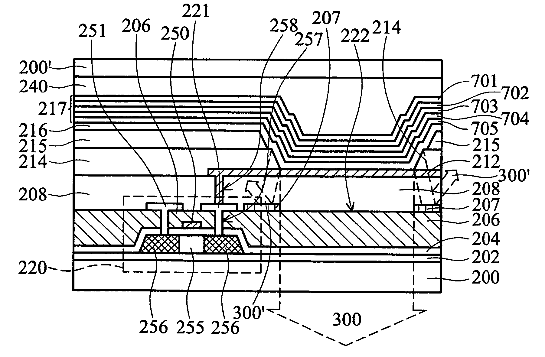
[0021] An OLED device of active matrix drive type according to this embodiment has at least one thin film transistor 220 and an organic LED device 160 provided on a substrate 200 for each pixel as shown in FIGS. 2 and 3D. FIG. 3D is a cross section of FIG. 2 taken along the line I-I′ in the direction indicated by the arrow.

[0022] The OLED device 160 includes a pixel electrode 2...


PUM


Abstract

An organic light-emitting device and method of fabricating the same. A substrate is provided. A first electrode is formed on the substrate. A light-emitting layer is disposed on the first electrode, and a second electrode is disposed on the light-emitting layer, wherein the first and second electrodes define a pixel area corresponding to an active light emitting area of the light-emitting layer. A light-shielding pattern is defined around the active light emitting area, to block stray light emitted by the light emitting-layer outside the active light emitting area.

Description

BACKGROUND OF THE INVENTION [0001] 1. Field of the Invention [0002] The present invention relates to an organic light-emitting device, and more particularly to an organic light-emitting device with a light-shielding layer and method of fabrication the same. [0003] 2. Description of the Related Art [0004] With recent development, organic light-emitting devices (OLEDs) have become a potential candidate to replace Liquid Crystal Displays (LCDs) for next-generation display. With their active light-emitting characteristics, OLEDs, unlike LCDS, do not require a backlight module to provide a light source, benefiting weight reduction. In addition, OLEDs have many distinguished advantages such as high contrast, fast response rate, high brightness, and wider viewing angle. The organic light-emitting diode uses an organic layer as an active layer, sandwiched between an anode and cathode electrodes to form a stacked layer. OLEDs are divided into small molecule and polymer device types according...

Claims


Application Information

Patent Timeline
IPC IPC(8): H01L27/32H01L35/24H01L51/52H05B33/00
CPCH01L51/5284H01L27/3244H10K59/12H10K59/8792H10K50/865
Inventor HSUEH, WEI-CHIEHTSAI, YAW-MING
Owner INNOLUX CORP
Learn More