Apparatus and method for over-voltage, under-voltage and over-current stress protection for transceiver input and output

a technology of transistor protection and under-voltage, applied in the direction of pulse automatic control, line-fault/interference reduction, baseband system details, etc., can solve the problems of internal chip transistors and external circuitry that operate at higher voltages, subject to various failure mechanisms, and the insulating properties of silicon dioxide in the cmos gate wear ou

Active Publication Date: 2005-09-01
AVAGO TECH INT SALES PTE LTD
View PDF7 Cites 10 Cited by
  • Summary
  • Abstract
  • Description
  • Claims
  • Application Information

AI Technical Summary

Benefits of technology

[0018] The present invention is directed to an apparatus and method for over-voltage, under-voltage and over-current stress protecti...

Problems solved by technology

However, there are still voltage level standards external to the chip that operate at higher voltages.
The interface between the internal chip transistors and the external circuitry that operate at higher voltages is often a problem due to the need to ensure that the internal chip transistors at the interface do not fail due to the higher voltages.
If these devices are implemented using CMOS transistors, they are subject to various failure mechanisms when a larger-than-foundry-specified maximum voltage is applied.
One such failure mechanism is Time Dependent Dielectric Breakdown (TDDB), where, if a large voltage is applied at a gate of a CMOS device, the insulating properties of the silicon dioxide in the CMOS gate wear out, leading to a formation of a conducting path between the gate and the substrate.
This then affects the gate-controlled conductivity properties of the transistor, causing circuit failure.
Another failure mechanism is hot carrier damage, where a transistor that is turned on is subjected to a drain-to-source voltage that is larger than the specified maximum.
However, this form of protection requires additional external diodes, which increases cost and introduces capacitive parastitics that can degrade high frequency operation.
Also, this solution does not solve the problem of interfacing to 5V or 3V systems when the internal chip circuitry is operating at, for example, 2.5V.
Also, it does not have a protection scheme for undervoltage stress conditions.
This can cause electron migration failure if the number of vias and contacts and the metal widths used to connect outp to the resistors, as well as resistor widths, are insufficient.
A thicker metal and resistor width for this signal would also mean greater area requirements, and hence increased cost.

Method used


Image

  • Apparatus and method for over-voltage, under-voltage and over-current stress protection for transceiver input and output
  • Apparatus and method for over-voltage, under-voltage and over-current stress protection for transceiver input and output
  • Apparatus and method for over-voltage, under-voltage and over-current stress protection for transceiver input and output

Examples


Embodiment Construction

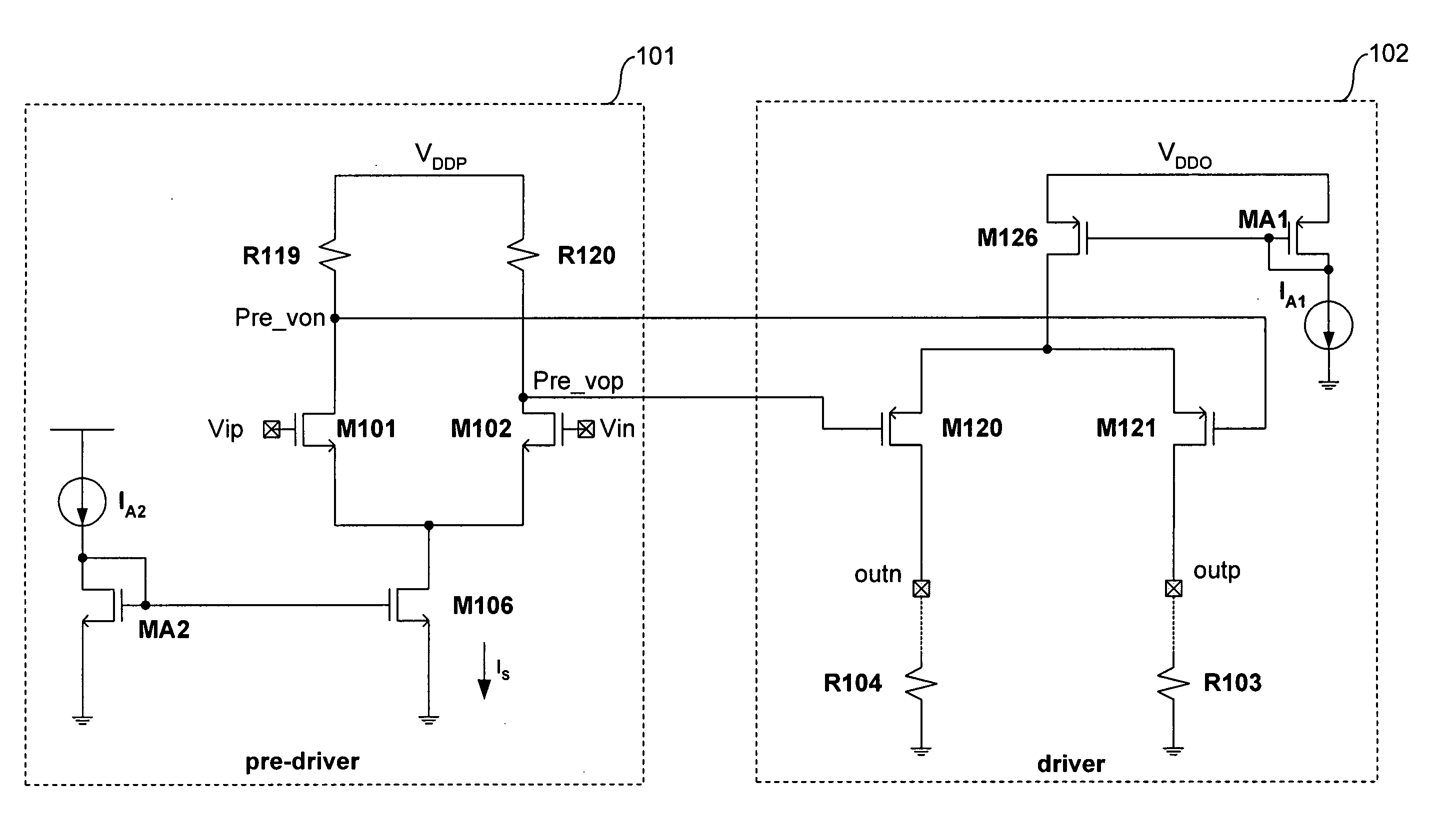
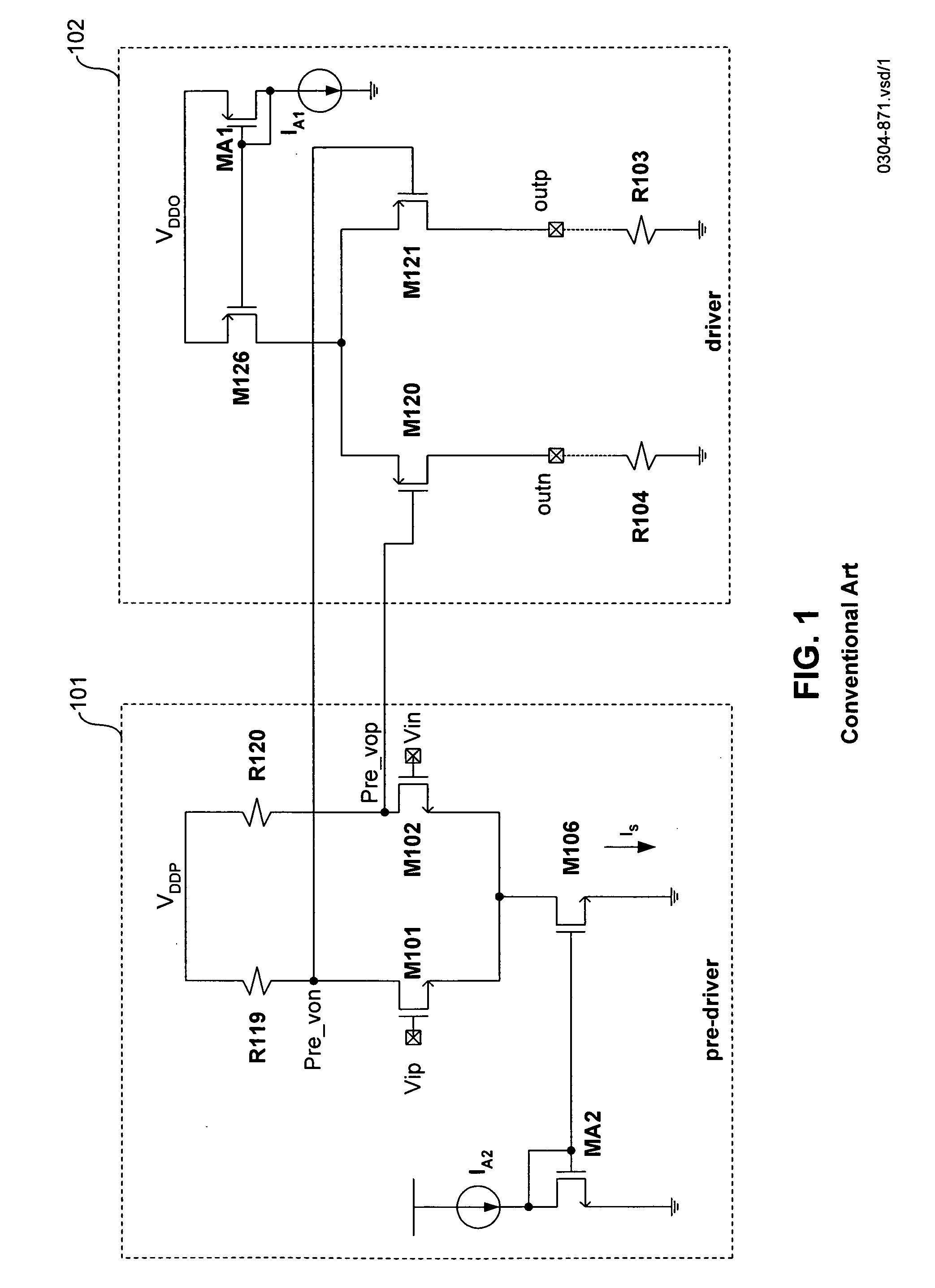
[0034] Reference will now be made in detail to the embodiments of the present invention, examples of which are illustrated in the accompanying drawings.

[0035] An “over-voltage stress condition” refers to a 5.25V power bus voltage being shorted to receiver input or transmitter output. An “under-voltage stress condition” refers to a −1V voltage in series with a 39 ohm resistor shorted to the receiver input or transmitter output.

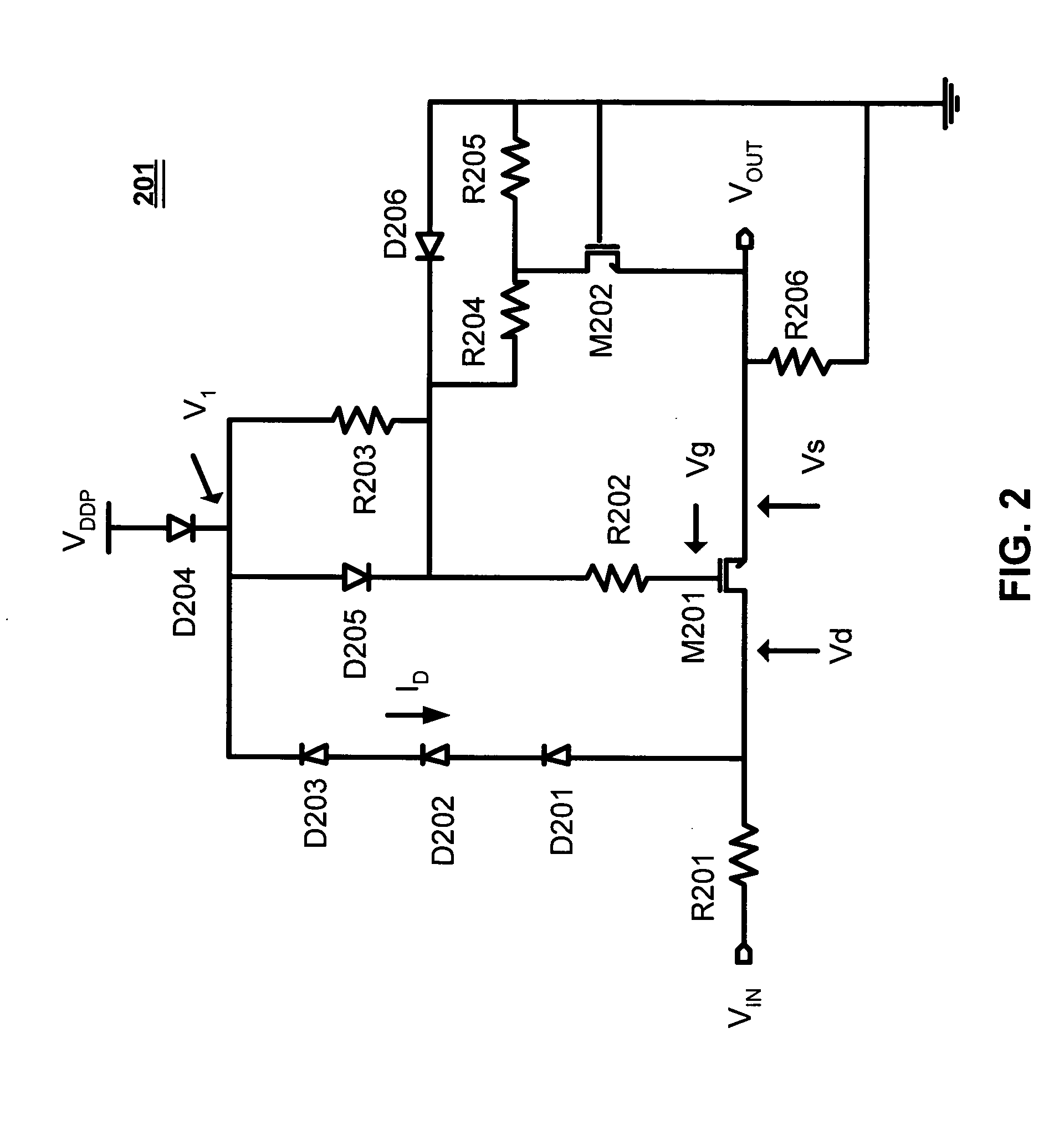
[0036] The following description of a receive input protection circuit 201 of FIG. 2 uses the following:

VDDP=2.5V, VDDO=3.3V, VDDC=1.2V.

[0037] Diode turn-on voltage-0.6˜0.8V, VDIO=0.6˜0.8V.

Vbusp=5.25V, Vbusn=−1V

[0038] Referring to FIG. 2, one embodiment of the proposed receive input protection circuit 201 includes the following:

[0039] An input transistor M201 in series with a resistor R201 is connected to an input pad Vin. The input transistor M201 acts as a transmission gate in normal operation, and as a voltage limiter during over-voltage and under-vol...


PUM


Abstract

A circuit for protection of a transceiver input includes an input transistor and a first resistor connected between the drain of the input transistor and an input node. A plurality of reverse-biased diodes connected between a supply voltage and the input node. An output node is connected to the source of the input transistor. A first forward-biased diode connected between the power supply and the plurality of reverse-biased transistors. A second forward-biased diode and a second resistor are connected between the first forward biased transistor and the gate of the input transistor. A pre-driver circuit includes first and second transistors forming a differential pair and driven by a differential input voltage. A third transistor is connected between sources of the first and second transistors and ground. First and second resistors are connected to drains of the first and second transistors, respectively. A fourth transistor is connected between a power supply voltage and the first and second resistors. Fifth and a sixth transistors are connected in series between the power supply voltage and the first and second resistors, wherein a node between the fifth and second transistors is connected to a gate of the fourth transistor.

Description

BACKGROUND OF THE INVENTION [0001] 1. Field of the Invention [0002] The present invention relates to method and apparatus for protecting transistors used in chip interface circuits, and more particularly, to the protection of transistors used in CMOS transceiver receive and transmit circuitry. [0003] 2. Related Art [0004] In modern submicron CMOS processes, minimum transistor dimensions have progressively become smaller over the years. This allows a faster operation, as well as the ability to integrate more functions on a chip. Transistor supply voltages have also been reduced, to maintain acceptable reliability of sub-micron transistors. However, there are still voltage level standards external to the chip that operate at higher voltages. Many legacy systems still work on 5V and 3.3V, although on-chip circuitry is required to work at 1.2V or 2.5V. The interface between the internal chip transistors and the external circuitry that operate at higher voltages is often a problem due to...

Claims


Application Information

Patent Timeline
IPC IPC(8): H01L27/02H02H3/20H04L25/08
CPCH04L25/08H01L27/0251
Inventor LEE, WEE TECKYUN, TUTEO, TIAN HWEE
Owner AVAGO TECH INT SALES PTE LTD
Why Eureka
Try Eureka