Semiconductor memory and method of manufacturing the same

Inactive Publication Date: 2005-09-01
INNOTECH CORP
View PDF8 Cites 9 Cited by
  • Summary
  • Abstract
  • Description
  • Claims
  • Application Information

AI Technical Summary

Benefits of technology

[0011] An object of the present invention is to provide

Problems solved by technology

Moreover, the following problems will occur as well.
Once the electrons are trapped, the electrons are localized in the silicon nitride layer 106b, so it is difficult to remove such electrons in the data erasing mode.
Moreover, the change in the channel length will

Method used


Image

  • Semiconductor memory and method of manufacturing the same
  • Semiconductor memory and method of manufacturing the same
  • Semiconductor memory and method of manufacturing the same

Examples


Embodiment Construction

[0048] The embodiment of the present invention is described in detail hereinafter with reference to the accompanying drawings.

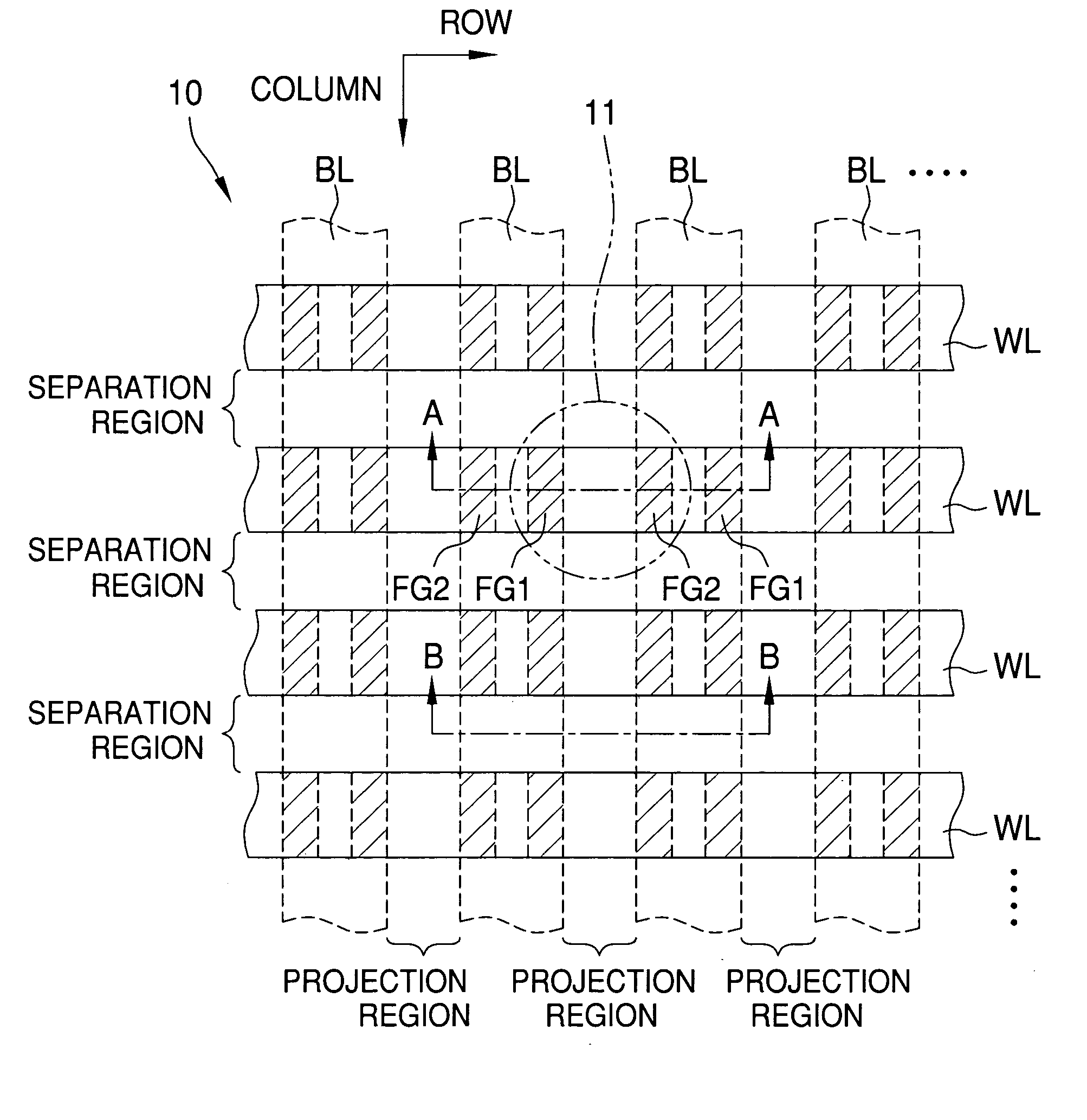
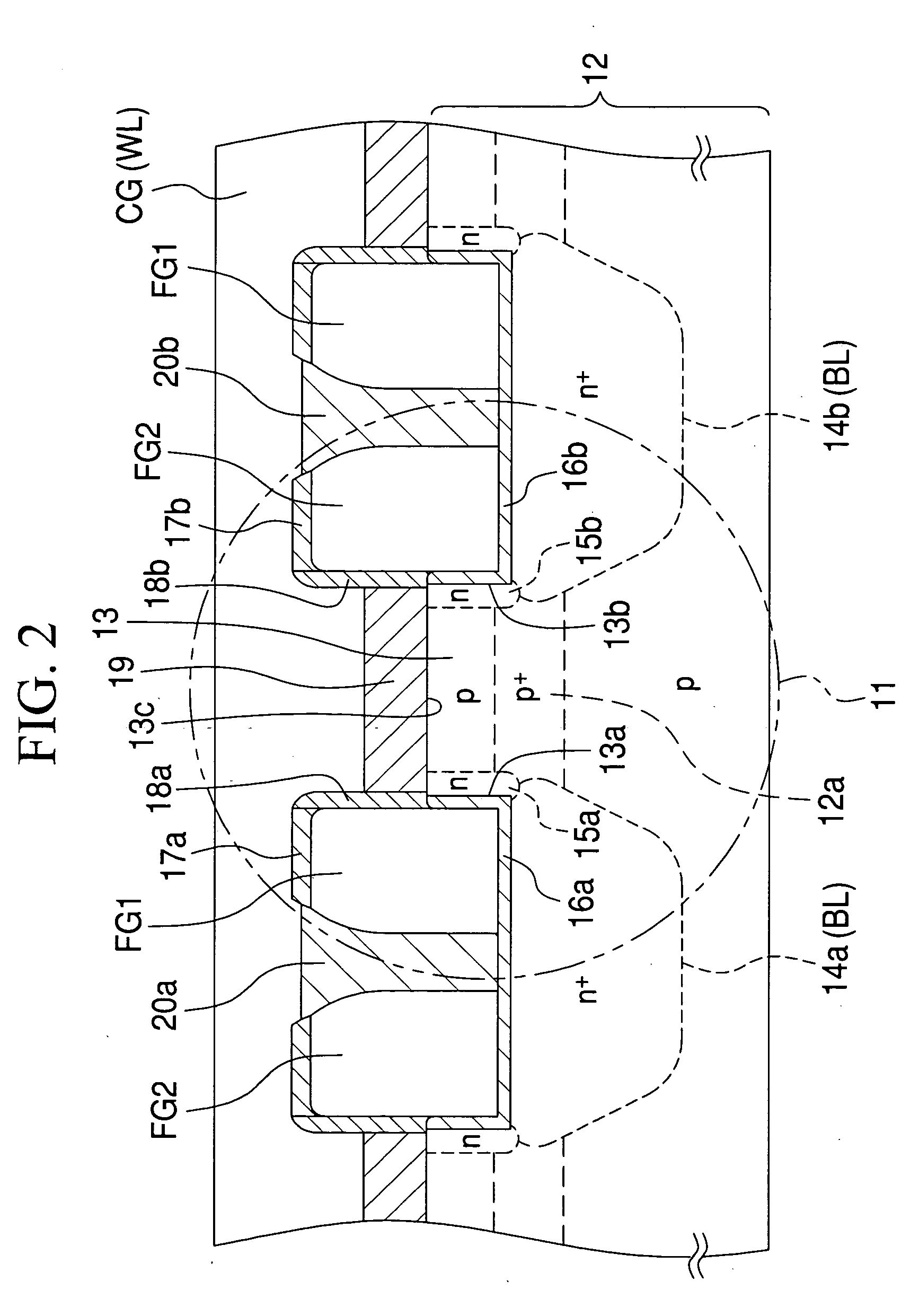
[0049] Referring to FIG. 1, a memory cell array 10 has a VGA (Virtual Ground Array) configuration in which plural bit lines (BL) and plural word lines (WL) are intersected. The bit line has a diffusion region that extends in a column direction. The word line is formed of conductive silicon that extends in a row direction. In the intersected area of the word line WL and the bit line BL, there are a pair of floating gates FG1 and FG2 that are electrically isolated from each other. The memory cell array 10 is in a form of a matrix having plural cell transistors 11. A single cell transistor 11 is depicted in a circled area of FIG. 1.

[0050] Between the adjacent bit lines BL, there is a projection 13 formed in a silicon substrate (semiconductor substrate) 12 (see FIG. 2). The projection 13 extends in the column direction, and a channel region is provided in the a...


PUM


Abstract

A semiconductor memory has plural cell transistors that are arranged in a matrix. The cell transistor comprises a silicon substrate, a control gate, a pair of electrically isolated floating gates. Plural projections are formed in the P type silicon substrate, and a pair of N type diffusion regions as the source and the drain is formed in both sides of the projection. The control gate faces the projection via a fourth insulation layer. The side surface of the floating gates faces the side surfaces of the projection via a first insulation layer, and faces the control gate via a third insulation layer. The floating gate faces the diffusion region via the first insulation layer.

Description

BACKGROUND OF THE INVENTION [0001] 1. Field of the Invention The present invention relates to a semiconductor memory having transistor cells each of which stores multiple bits, and a method of manufacturing such semiconductor memory. [0002] 2. Description of Background Art [0003] Recently, nonvolatile semiconductor memories such as flash memories are widely applied to electronic appliances such as a mobile telephone. In order to promote size reduction and larger information capacity of the electronic appliances, it is required to miniaturize the semiconductor memory and increase the storage capacity of the semiconductor memory. Thus, there should preferably be implements the multiple-bit configuration of a cell transistor that allows two or more bits of information to be stored in a single cell transistor. The nonvolatile semiconductor memory described in US 2004 / 0169219 A1, filed by the assignee of the present application, has cell transistors each of which comprises a pair of floa...

Claims


Application Information

Patent Timeline
IPC IPC(8): G11C11/34G11C16/04H01L21/8247H01L27/115H01L29/788H01L29/792
CPCG11C16/0408H01L29/7887H10B69/00H10B41/30
Inventor MIIDA, TAKASHI
Owner INNOTECH CORP
Why Eureka
Try Eureka