Method of forming thin film pattern, method of manufacturing device, electro-optical apparatus and electronic apparatus

a manufacturing device and thin film technology, applied in the direction of non-linear optics, identification means, instruments, etc., can solve the problems of large-scale equipment, high manufacturing cost, complicated processing, etc., and achieve the effect of suppressing the generation of bulges

Inactive Publication Date: 2005-09-01
SEIKO EPSON CORP
View PDF8 Cites 27 Cited by
  • Summary
  • Abstract
  • Description
  • Claims
  • Application Information

AI Technical Summary

Benefits of technology

[0032] According to this aspect, because a residue processing step is provided in which residue is removed, it is possible to place the functional liquid uniformly on the substrate. Accordingly, the generation of bulges is suppressed, and the thin film pattern that is formed is able to avoid the occurrence of malfunctions such as broken wires and the like. Accordingly, it is possible to manufacture an active matrix substrate that has desired characteristics.

Problems solved by technology

This photolithographic method requires large scale equipment such as a vacuum apparatus and also requires complicated processing.
Moreover, the material utilization efficiency is approximately several percent and it is necessary to scrap the greater part thereof, so that manufacturing costs are high.
However, in the above described conventional technology, the following problem exists.
When the functional liquid is placed on the substrate in order to form the wiring pattern, if there is any residue on the substrate, then, in some cases, the functional liquid may not be placed uniformly on the substrate which becomes a cause of the occurrence of malfunctions such as bulges and wiring breakages

Method used


Image

  • Method of forming thin film pattern, method of manufacturing device, electro-optical apparatus and electronic apparatus
  • Method of forming thin film pattern, method of manufacturing device, electro-optical apparatus and electronic apparatus
  • Method of forming thin film pattern, method of manufacturing device, electro-optical apparatus and electronic apparatus

Examples


experiment example

(Experiment Example)

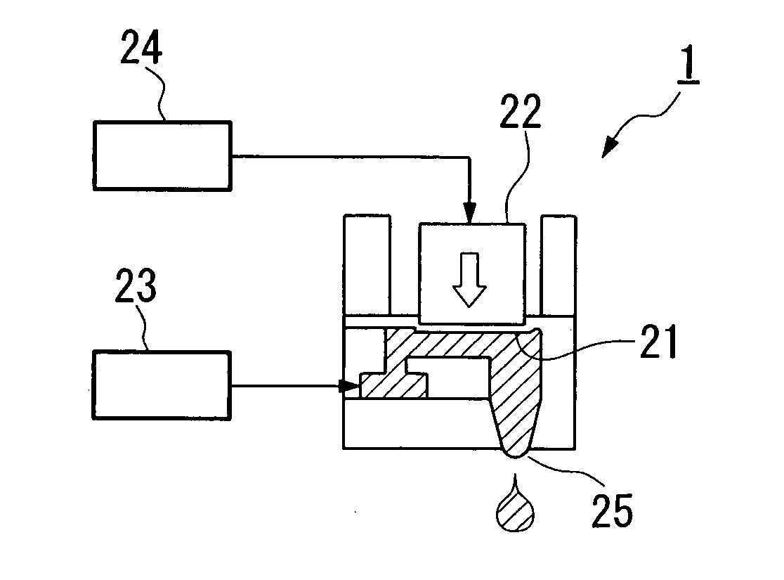
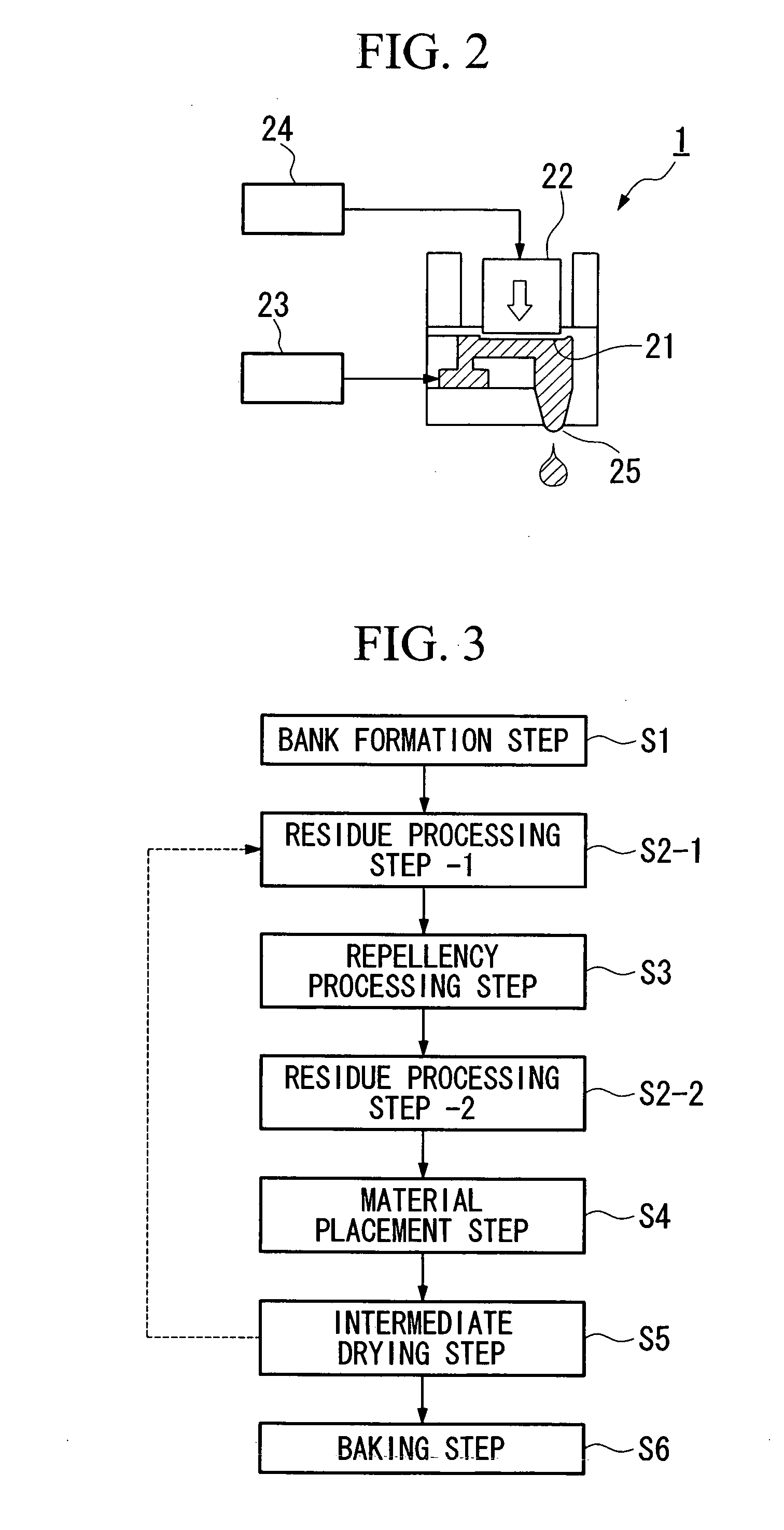
[0107] A HMDS layer 32 was formed on the substrate P. Banks B were then formed thereon. Next, without hydrofluoric acid processing being performed, O2 plasma processing was performed on the substrate P using the above described plasma processing apparatus. The processing conditions were set as a plasma power of 550 W, an oxygen gas flow rate of 100 mL / min, and a He gas flow rate of 10 L / min. The rate of movement of the specimen table 40 of the plasma processing apparatus were varied in sequence from 1 mm / sec to 2 mm / sec to 5 mm / sec. The contact angle between pure water and the bottom portions 35 (i.e. the exposed portions of the substrate P) between the banks after the O2 plasma processing were then measured. As a result, it was found that, when the table movement rate was 1 mm / sec, a substrate in which the contact angle was approximately 59 degrees before the O2 plasma processing was changed to a contact angle of 10 degrees or less after the O2 plasma processing...


PUM

PropertyMeasurementUnit
particle diameteraaaaaaaaaa
diameteraaaaaaaaaa
diameteraaaaaaaaaa

Abstract

A method of forming a thin film pattern by placing a functional liquid on a substrate, includes a bank formation step of forming banks in accordance with the thin film pattern on the substrate, a residue processing step of removing residue between the banks, and a material placement step of placing the functional liquid between the banks removed the residue.

Description

BACKGROUND OF THE INVENTION [0001] 1. Field of the Invention [0002] The present invention relates to a method of filming a thin film pattern and a method of manufacturing a device, and to an electro-optical apparatus and an electronic apparatus. [0003] Priority is claimed on Japanese Patent Application No. 2003-98274, filed Apr. 1, 2003 and Japanese Patent Application No. 2004-70834, filed Mar. 12, 2004, the contents of which are incorporated herein by reference. [0004] 2. Description of Related Art [0005] A photolithographic method, for example, is employed in the manufacture of devices having wiring such as electronic circuits and integrated circuits. In this photolithographic method, a photosensitive material known as resist is coated on a substrate on which an electroconductive film has been coated in advance. A circuit pattern is then irradiated thereon and the resist is developed. The electroconductive film is then etched in accordance with the resist pattern so as to form a t...

Claims


Application Information

Patent Timeline
Patent Type & Authority Applications(United States)
IPC IPC(8): B05D1/32B05D3/04B05D3/06G02F1/13B05D7/00G09F9/00H01L21/00H01L21/02H01L21/20H01L21/28H01L21/288H01L21/3205H01L21/321H01L21/336H01L21/768H01L21/77H01L21/84H01L27/32H01L29/786H01L51/00H01L51/50H05B33/14H05K3/10H05K3/12
CPCH01L21/288H01L21/76802H01L21/76814H01L21/76826H01L21/76829H01L21/76877H01L27/1292H01L51/0005H05K3/125H05K3/1258H05K2201/09909H05K2203/013H05K2203/1173H01L27/3244H10K59/12H10K71/135H01L21/28
Inventor HIRAI, TOSHIMITSU
Owner SEIKO EPSON CORP
Why Eureka
Try Eureka