Method of forming barrier layer with reduced resistivity and improved reliability in copper damascene process

a damascene and barrier layer technology, applied in the direction of semiconductor/solid-state device manufacturing, basic electric elements, electric apparatus, etc., can solve the problems of inadequate step coverage of damascene openings with barrier layer deposition methods, degrading damascene electrical resistivity, and low-k materials, so as to improve the electrical resistance and improve the resistance to copper migration

Active Publication Date: 2005-09-01
TAIWAN SEMICON MFG CO LTD
View PDF10 Cites 28 Cited by
  • Summary
  • Abstract
  • Description
  • Claims
  • Application Information

AI Technical Summary

Benefits of technology

[0008] To achieve the foregoing and other objects, and in accordance with the purposes of the present invention, as embodied and broadly described here...

Problems solved by technology

One problem with using porous low-k materials together with using copper as the metal filling in a copper damascene process is the susceptibility of the low-k materials to copper diffusion into the IMD layers, which has the effect of altering the dielectric constant of the IMD layer and degrading damascene electrical resistivity.
As device characteristic dimensions have decreased below about 0.25 microns and lower including less than about 0.17 microns, adequate step c...

Method used


Image

  • Method of forming barrier layer with reduced resistivity and improved reliability in copper damascene process
  • Method of forming barrier layer with reduced resistivity and improved reliability in copper damascene process
  • Method of forming barrier layer with reduced resistivity and improved reliability in copper damascene process

Examples


Embodiment Construction

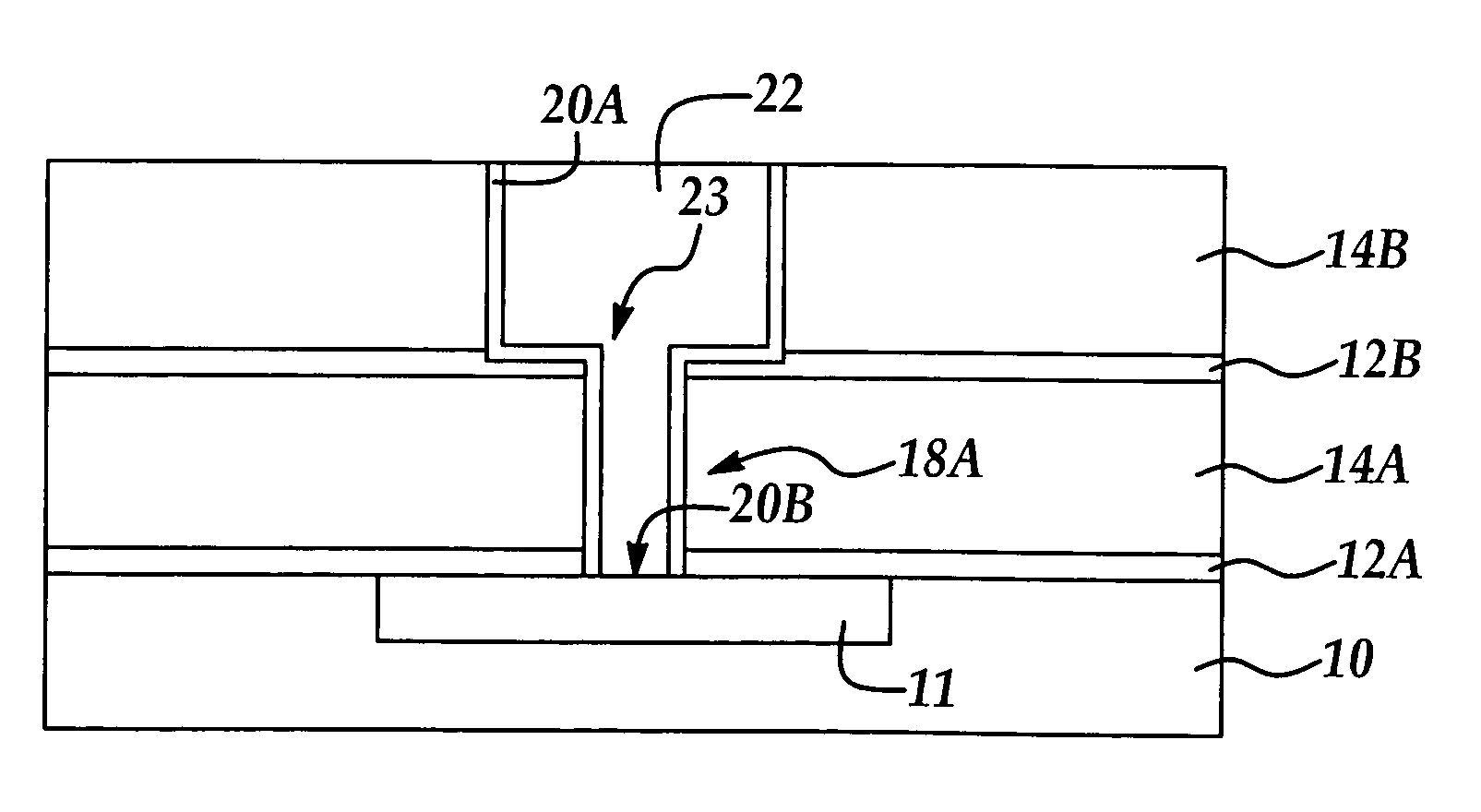
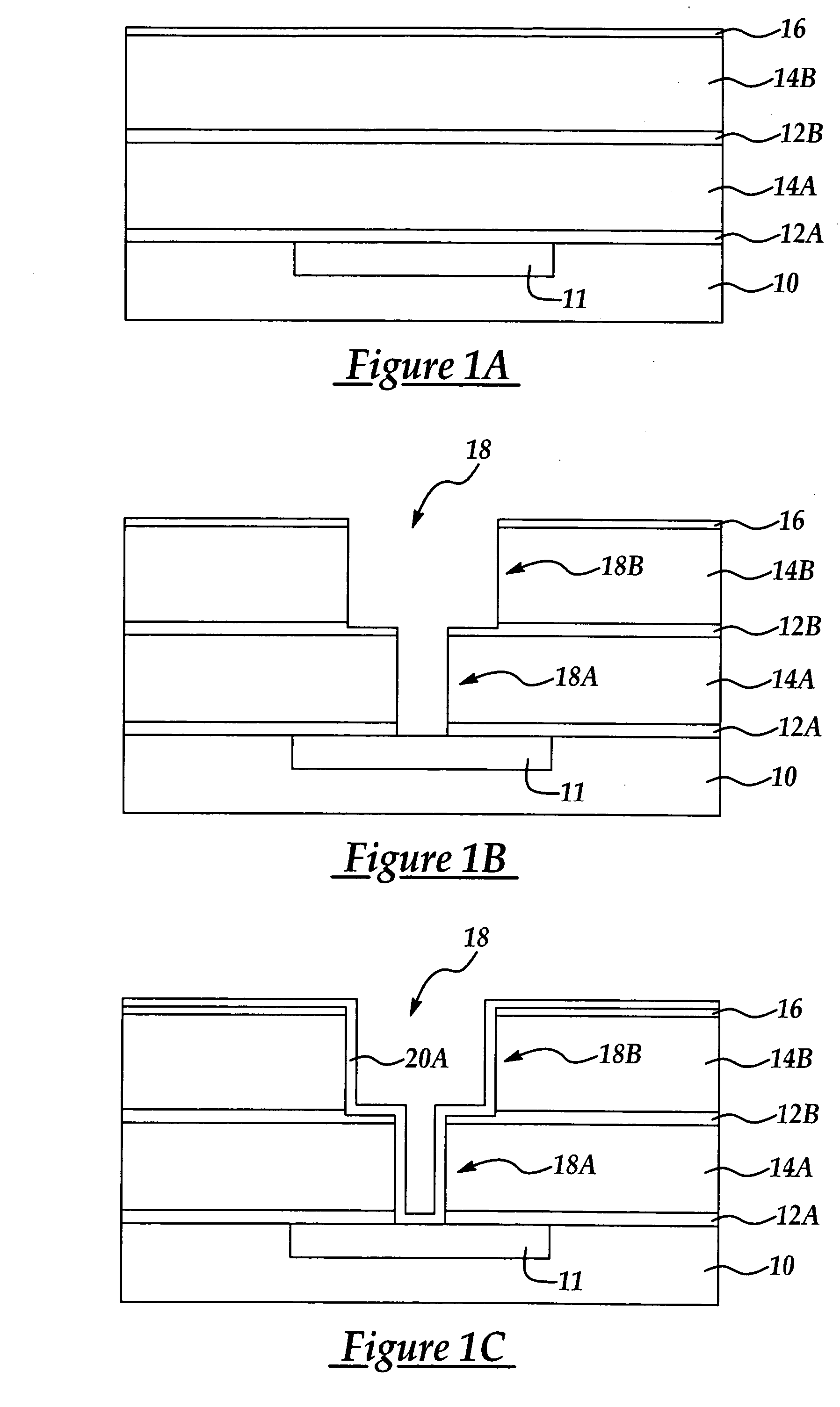
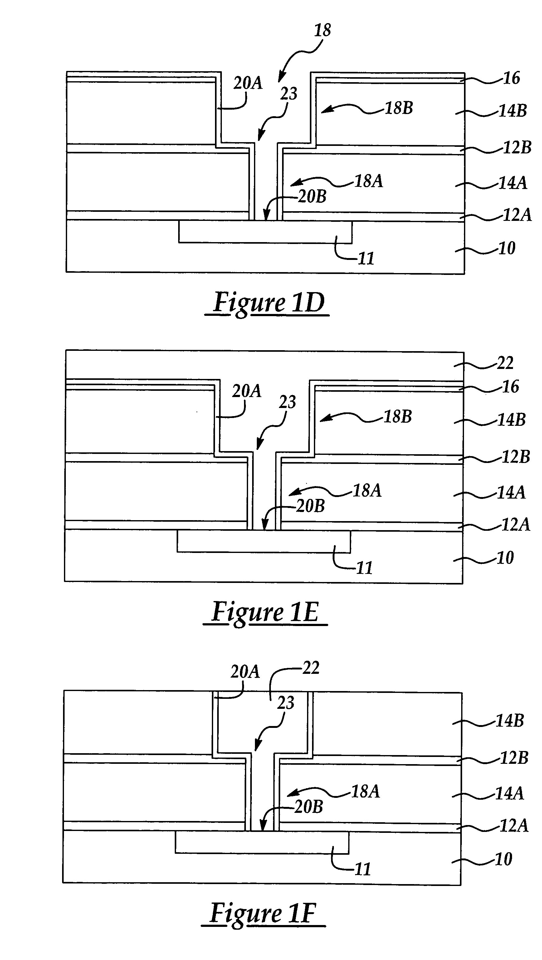
[0014] Although the present invention is explained by reference to an exemplary dual damascene formation process, it will be that the method of the present invention applies generally to the formation of damascenes including dual damascenes whereby stacked multi-layer inter-metal dielectric (IMD) layers, also referred to as an inter-layer dielectric (ILD), may be formed with an intervening etch stop layer to improve barrier layer coverage, resistance to copper electro-migration, and improved electrical performance and reliability. Although the method of the present invention is particularly advantageous in forming copper damascenes with characteristic dimensions of less than about 0.17 microns, and aspect ratios (depth to diameter / width) of greater than about 6 to 1, it will be appreciated that the method of the present invention may be adapted to larger characteristic dimension damascene processes.

[0015] By the term damascene is meant any metal filled opening formed in a dielectri...


PUM


Abstract

A method for forming a copper dual damascene with improved copper migration resistance and improved electrical resistivity including providing a semiconductor wafer including upper and lower dielectric insulating layers separated by a middle etch stop layer; forming a dual damascene opening extending through a thickness of the upper and lower dielectric insulating layers wherein an upper trench line portion extends through the upper dielectric insulating layer thickness and partially through the middle etch stop layer; blanket depositing a barrier layer including at least one of a refractory metal and refractory metal nitride to line the dual damascene opening; carrying out a remote plasma etch treatment of the dual damascene opening to remove a bottom portion of the barrier layer to reveal an underlying conductive area; and, filling the dual damascene opening with copper to provide a substantially planar surface.

Description

FIELD OF THE INVENTION [0001] This invention generally relates to semiconductor device manufacturing methods and more particularly to a method for forming copper damascenes with reduced electrical resistivity and improved reliability. BACKGROUND OF THE INVENTION [0002] In forming damascene structures in integrated circuit manufacturing processes, barrier layer uniformity is critical for achieving acceptable copper diffusion resistance and for achieving electrical resistances within required IC performance standard constraints. A damascene opening, for example a dual damascene opening is formed in an inter-metal dielectric insulating layer by a series of photolithographic patterning and etching processes, followed by formation of a barrier layer and a metal filling process. [0003] Increasingly, low-K layers are required to reduce signal delay and power loss effects as integrated circuit devices are scaled down. One way this has been accomplished has been to introduce porosity or dopa...

Claims


Application Information

Patent Timeline
IPC IPC(8): H01L21/44H01L21/768
CPCH01L21/76807H01L21/76865H01L21/76862H01L21/76844
Inventor CHEN, KEI-WEITSAO, JUNG-CHIHLIU, CHI-WENCHEN, JCHUNG-CHANGCHANG, SHIH-TZUNGLIN, SHIH-HOLIN, YU-KUWANG, YING-LANG
Owner TAIWAN SEMICON MFG CO LTD
Why Eureka
Try Eureka