Light emitting device

a technology of light emitting devices and light sources, which is applied in the direction of semiconductor devices, basic electric elements, electrical equipment, etc., can solve the problems of high energy consumption, insufficient heat radiation, and the speed of response (operation) of the element, and achieve high reliability and high intensity

Inactive Publication Date: 2005-09-08
NICHIA CORP
View PDF7 Cites 33 Cited by
  • Summary
  • Abstract
  • Description
  • Claims
  • Application Information

AI Technical Summary

Benefits of technology

[0012] It is an object of the invention to provide a thin surface mounting type light emitting device which has high reliability and capable of emitting the light with high intensity.
[0013] The light emitting device according to an aspect of the present invention comprises a light emitting element, a metal package having a recess part for housing the light emitting element and a base part which has one or more through holes, one or more lead electrode pins which penetrate the through holes and are separated from the through holes by a insulating member respectively. In the light emitting device, the bottom faces of the lead electrode pins project out from the bottom face of the base part and are positioned on the same plane including an outer bottom face of the recess part. With this configuration, the light emitting device which has a good mountability (can be mounted easily) and high reliability can be obtained.
[0014] It is preferable that the upper faces of the lead electrode pins project out from the upper face of the base part to improve the accuracy in bonding positions.

Problems solved by technology

However, such light emitting devices will be required to withstand more severe environment as their applications expand.
However, that heat radiation is not enough.
Therefore, the speed of response (operation) of the element and the resin covering the element deteriorate by raising the temperature of the light emitting element arose from insufficiently heat radiation.

Method used


Image

  • Light emitting device
  • Light emitting device
  • Light emitting device

Examples


example 1

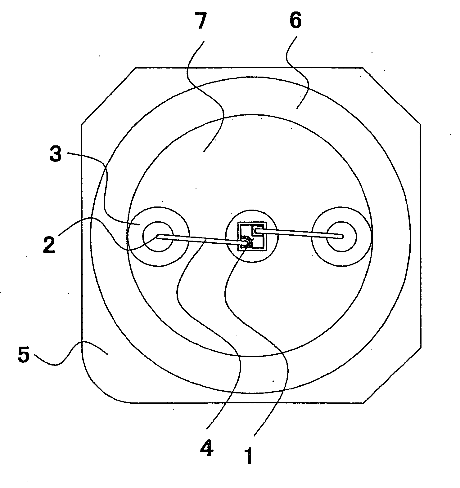
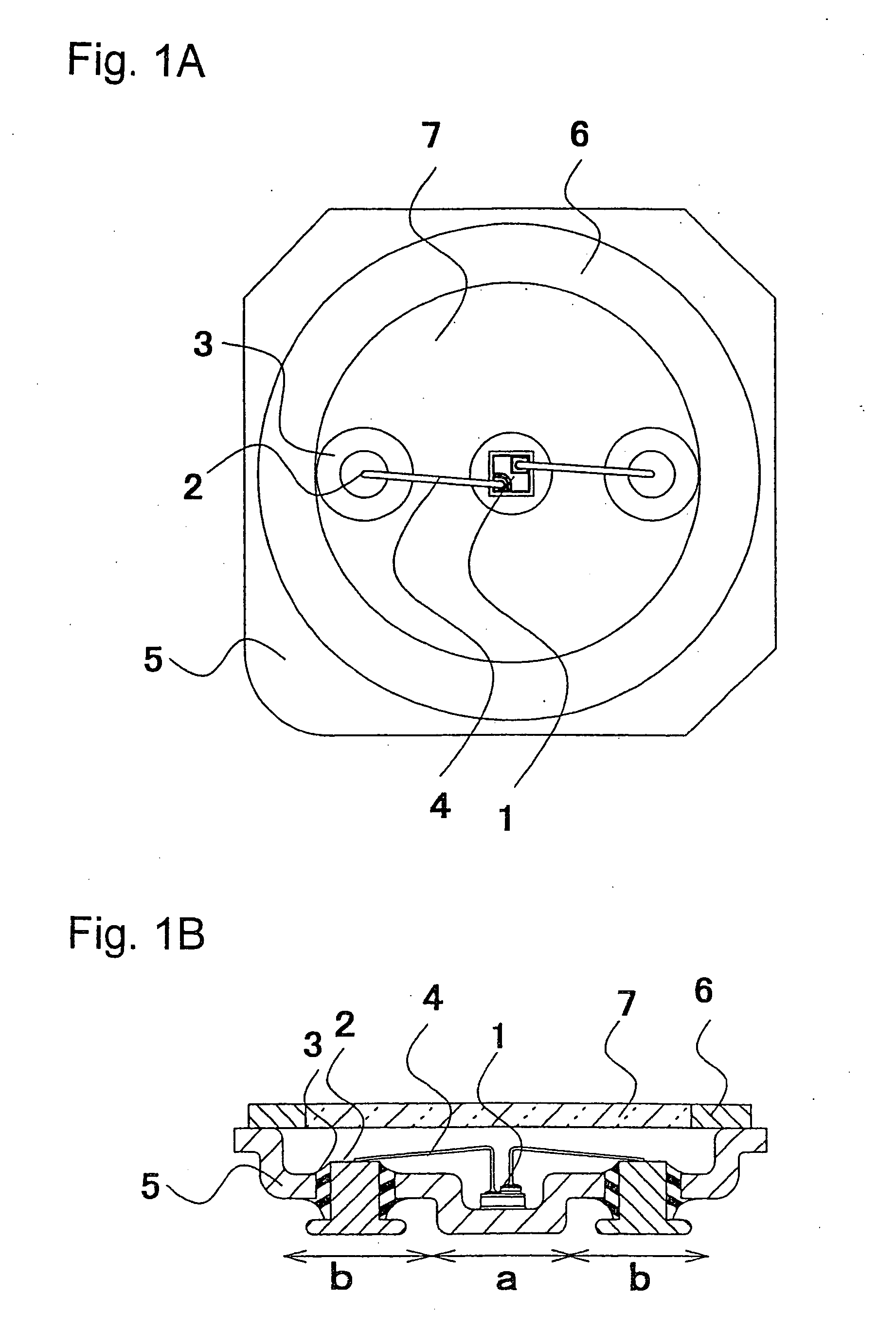
[0116] The light emitting device of surface mounting type shown in FIGS. 1A and 1B is made. The LED chip is a nitride semiconductor device having an active layer made of In0.2Ga0.8N of which peak wavelength is 475 nm in visible light. The LED chip is produced by growing the nitride semiconductors on a sapphire substrate by MOCVD method using TMG(trimethyl-gallium) gas, TMI(trimethyl-indium) gas, nitrogen gas, dopant gas and carrier gas. The n-type nitride semiconductor can be made using the SiH4 gas as a dopant gas and p-type nitride semiconductor can be made using the Cp2Mg as a dopant gas.

[0117] The LED chip has a structure constituted by laminating an n-type GaN layer of undoped nitride semiconductor, an n-type GaN (doped with Si) layer which is a contact layer for forming an n-type electrode, an n-type GaN layer of undoped nitride semiconductor and a light emitting layer in turn on a sapphire substrate. The light emitting layer is a multi quantum well structure composed of five...

example 2

[0125] A light emitting device of Example 2 is the same as the light emitting device of Example 1 except that a package of iron of which base part has a thicker thickness than that of the bottom part of the recess is used instead of the covar package. In the light emitting device of Example 2, the heat generated by the light emitting element can be radiated more efficiently than Example 1. Moreover, the light emitting device of Example 2 has a mechanical strength higher than that of the light emitting element of Example 1. Therefore, the reliability and the productivity are improved, so the light emitting device which can maintain a high power output by large current for a long time can be produced with good productivity.

example 3

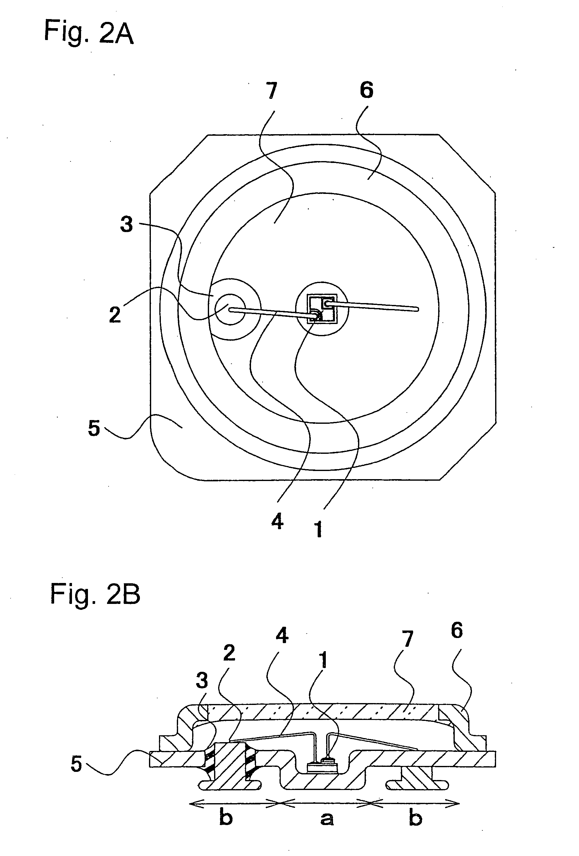
[0126] A light emitting device of Example 3 is the same as the light emitting device of Example 2 except that a package of iron of which recess has a tapered inner wall (shown in FIG. 4) is used. In the light emitting device of Example 3, the mechanical strength and the output power of emitted light can be improved 15%.


PUM


Abstract

A light emitting device comprises a light emitting element, a metal package having a recess part for housing the light emitting element and a base part which has one or more through holes, and one or more lead electrode pins which penetrate the through holes and are separated from the through holes by an insulating member respectively. The bottom faces of the lead electrode pins project out from the bottom face of the base part and are positioned on a same plane including an outer bottom face of the recess part. With this configuration, the light emitting device has a good heat radiating characteristic and high mechanical strength.

Description

[0001] This application is a divisional of co-pending application Ser. No. 10 / 475,001 filed on Oct. 16, 2003 and for which priority is claimed under 35 U.S.C. § 120. application Ser. No. 10 / 475,001 is the national phase of PCT International Application No. PCT / JP02 / 03759 filed on Apr. 16, 2002 under 35 U.S.C. § 371. The entire contents of each of the above-identified applications are hereby incorporated by reference. This application also claims priority of Application No. 2001-118458 filed in Japan on Apr. 17, 2001 under 35 U.S.C. § 119 and Application 2002-024208 filed in Japan on Jan. 31, 2002.TECHNICAL FIELD [0002] The present invention relates to light emitting devices which are utilized as kinds of light sources for backlights, displays and lightings, and particularly relates to light emitting devices having high reliability. BACKGROUND ART [0003] Recently, a high luminance and high power light emitting semiconductor device, and a small sized and high sensitivity light emittin...

Claims


Application Information

Patent Timeline
Patent Type & Authority Applications(United States)
IPC IPC(8): H01L27/15H01L33/50H01L33/32H01L33/64
CPCH01L24/49H01L33/483H01L33/507H01L33/62H01L33/642H01L2224/48091H01L2224/4823H01L2224/48465H01L2224/49107H01L2224/49113H01L2224/73265H01L2924/01004H01L2924/01012H01L2924/01013H01L2924/0102H01L2924/01029H01L2924/0103H01L2924/01032H01L2924/01038H01L2924/01039H01L2924/01047H01L2924/01049H01L2924/0105H01L2924/01052H01L2924/01056H01L2924/01057H01L2924/01058H01L2924/01059H01L2924/0106H01L2924/01063H01L2924/01073H01L2924/01078H01L2924/01079H01L2924/01082H01L2924/01005H01L2924/01006H01L2924/01019H01L2924/01021H01L2924/01024H01L2924/01033H01L2924/01065H01L2924/01066H01L2924/01074H01L2924/01075H01L2924/014H01L2924/10329H01L2224/32245H01L2224/45124H01L2224/45139H01L2224/45144H01L2924/12041H01L24/45H01L2924/00014H01L2924/00H01L2924/351H01L2924/181H01L2924/12042H01L2924/12036H01L24/48H01L2224/45015H01L2924/207
Inventor SUENAGA, RYOMA
Owner NICHIA CORP
Why Eureka
Try Eureka