Semiconductor device and manufacturing method thereof

a technology of semiconductors and semiconductors, applied in the direction of digital transmission, error prevention, transmission, etc., can solve the problems of increased switching time and deteriorated forward voltag

Active Publication Date: 2005-09-08
SEMICON COMPONENTS IND LLC
View PDF11 Cites 36 Cited by
  • Summary
  • Abstract
  • Description
  • Claims
  • Application Information

AI Technical Summary

Problems solved by technology

Accordingly, there arises a problem that the forward voltage is deteriorated and switching time is increased.

Method used


Image

  • Semiconductor device and manufacturing method thereof
  • Semiconductor device and manufacturing method thereof
  • Semiconductor device and manufacturing method thereof

Examples


Embodiment Construction

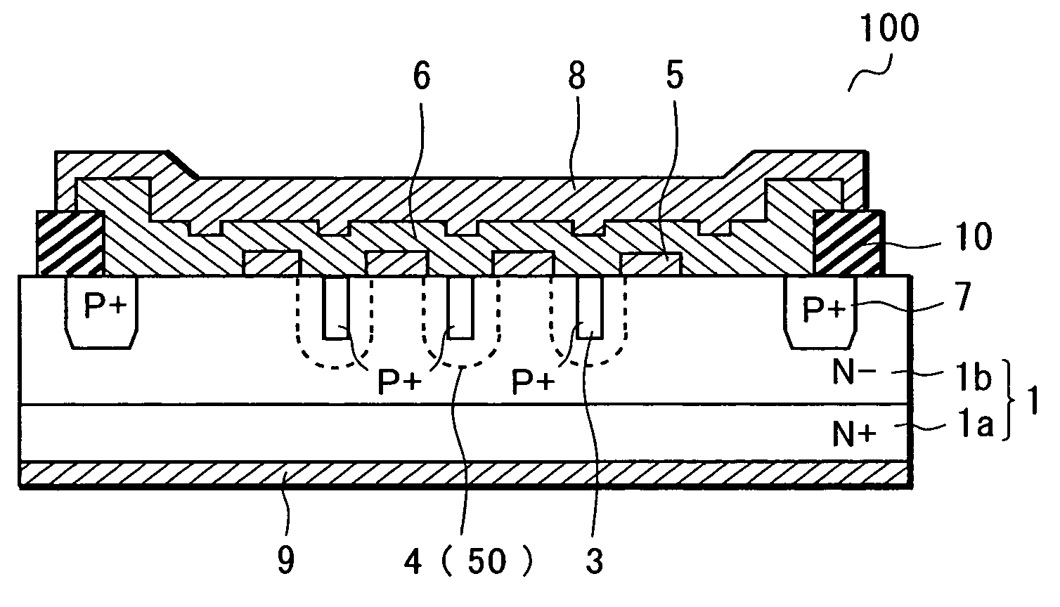
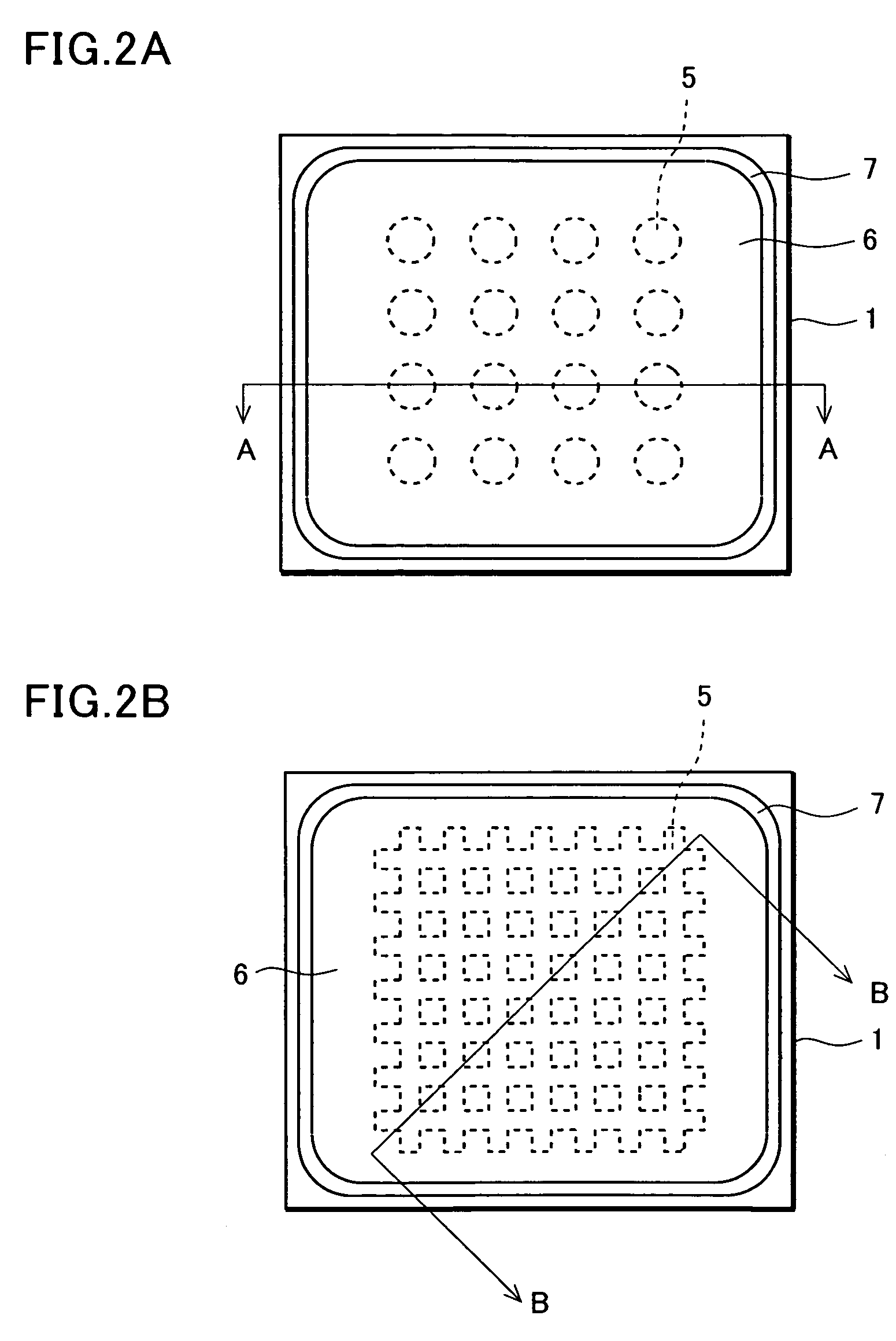
[0021] With reference to FIGS. 1 to 5, an embodiment of the present invention will be described in detail.

[0022]FIG. 1 and FIGS. 2A and 2B show a Schottky barrier diode according to the embodiment of the present invention. FIG. 1 is a cross-sectional view, and FIGS. 2A and 2B are plan views. Moreover, FIG. 1 corresponds to a cross-sectional view along the line A-A in FIG. 2A or a cross-sectional view along the line B-B in FIG. 2B. Furthermore, in FIGS. 2A and 2B, an anode electrode on a surface of a substrate is omitted. The Schottky barrier diode 100 of the preferred embodiment includes a one conductivity type semiconductor substrate 1, opposite conductivity type regions 3, a first metal layer 5, and a second metal layer 6.

The semiconductor substrate 1 is obtained by laminating a N− type epitaxial layer 1b on a N+ type semiconductor substrate 1a.

[0023] The opposite conductivity type regions 3 are a plurality of P+ type regions provided in the epitaxial layer 1b. P+ type impurit...


PUM


Abstract

Since VF and IR characteristics of a Schottky barrier diode are in a trade-off relationship, there has heretofore been a problem that an increase in a leak current is unavoidable in order to realize a low VF. Moreover, there has been a known structure which suppresses the leak current in such a manner that a depletion layer is spread by providing P+ regions and a pinch-off effect is utilized. However, in reality, it is difficult to completely pinch off the depletion layer. P+ type regions are provided, and a low VF Schottky metal layer is allowed to come into contact with the P+ type regions and depletion regions therearound. A low IR Schottky metal layer is allowed to come into contact with a surface of a N type substrate between the depletion regions. When a forward bias is applied, a current flows through the metal layer of low VF characteristic. When a reverse bias is applied, a current path narrowed by the depletion regions is formed only in the metal layer portion of low IR characteristic. Thus, a low VF and low IR Schottky barrier diode can be realized.

Description

BACKGROUND OF THE INVENTION [0001] 1. Field of the Invention [0002] The present invention relates to a semiconductor device and a manufacturing method thereof, more particularly relates to a semiconductor device capable of improving low forward voltage and low leak current characteristics of a Schottky barrier diode, and a manufacturing method thereof. [0003] 2. Description of the Related Art [0004]FIGS. 6A and 6B show a conventional Schottky barrier diode 110. FIG. 6A is a plan view, and FIG. 6B is a cross-sectional view along the line C-C in FIG. 6A. [0005] A substrate 21 is obtained by laminating a N− type epitaxial layer 21b on a N+ type semiconductor substrate 21a. On the N− type epitaxial layer 21b which is exposed through an opening of an insulating film 60, a Schottky metal layer 25 is provided, which forms a Schottky junction with a surface thereof. This metal layer is, for example, Ti. Furthermore, an Al layer to be an anode electrode 28 by covering the entire metal layer ...

Claims


Application Information

Patent Timeline
Patent Type & Authority Applications(United States)
IPC IPC(8): H01L29/423H01L29/872H01L29/47
CPCH01L29/66143H01L29/872H01L29/861H04L1/1812H04L1/1877H04L1/1607H04L1/1883
Inventor SOUMA, TADAAKINATSUME, TADASHI
Owner SEMICON COMPONENTS IND LLC
Why Eureka
Try Eureka