Electroluminescence display device

Active Publication Date: 2005-09-15
SAMSUNG DISPLAY CO LTD
View PDF10 Cites 53 Cited by
  • Summary
  • Abstract
  • Description
  • Claims
  • Application Information

AI Technical Summary

Benefits of technology

[0018] The present invention provides an electroluminescent display device that has an increased ratio of display area to

Problems solved by technology

In an organic/inorganic electroluminescent display device, particularly, in an active matrix type organic/inorganic electroluminescent device, a problem is presented that a proportion of a display area including pixels relative to a substrate is reduced due to lay-out of various driving circuits and wirings substrate.
This lowers a proportion of the display area 20 relative to the overall size of the display device, resulting in an increase in dead space (i.e. non-emissive region).
This design, however, increases

Method used


Image

  • Electroluminescence display device
  • Electroluminescence display device
  • Electroluminescence display device

Examples


Embodiment Construction

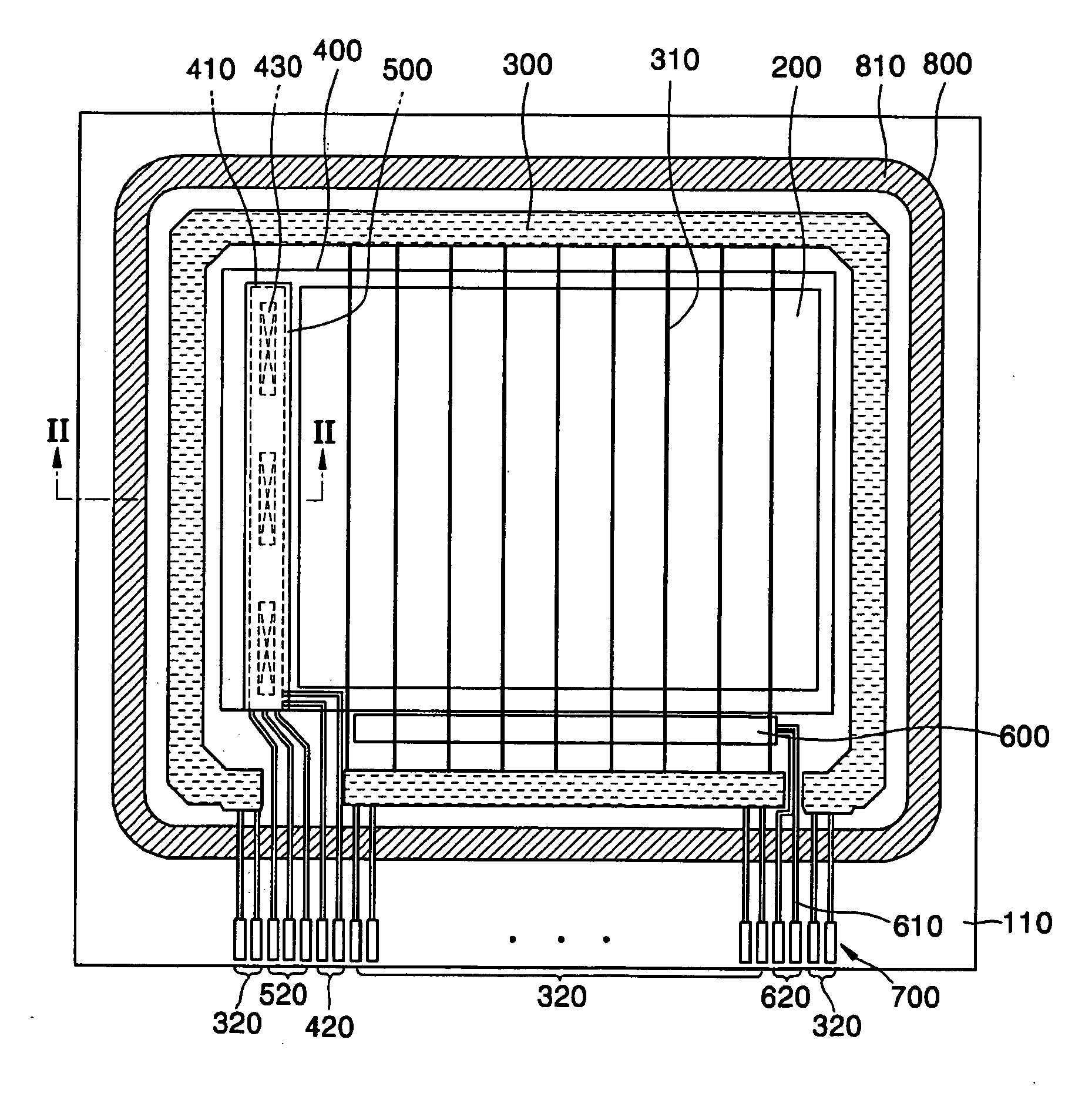
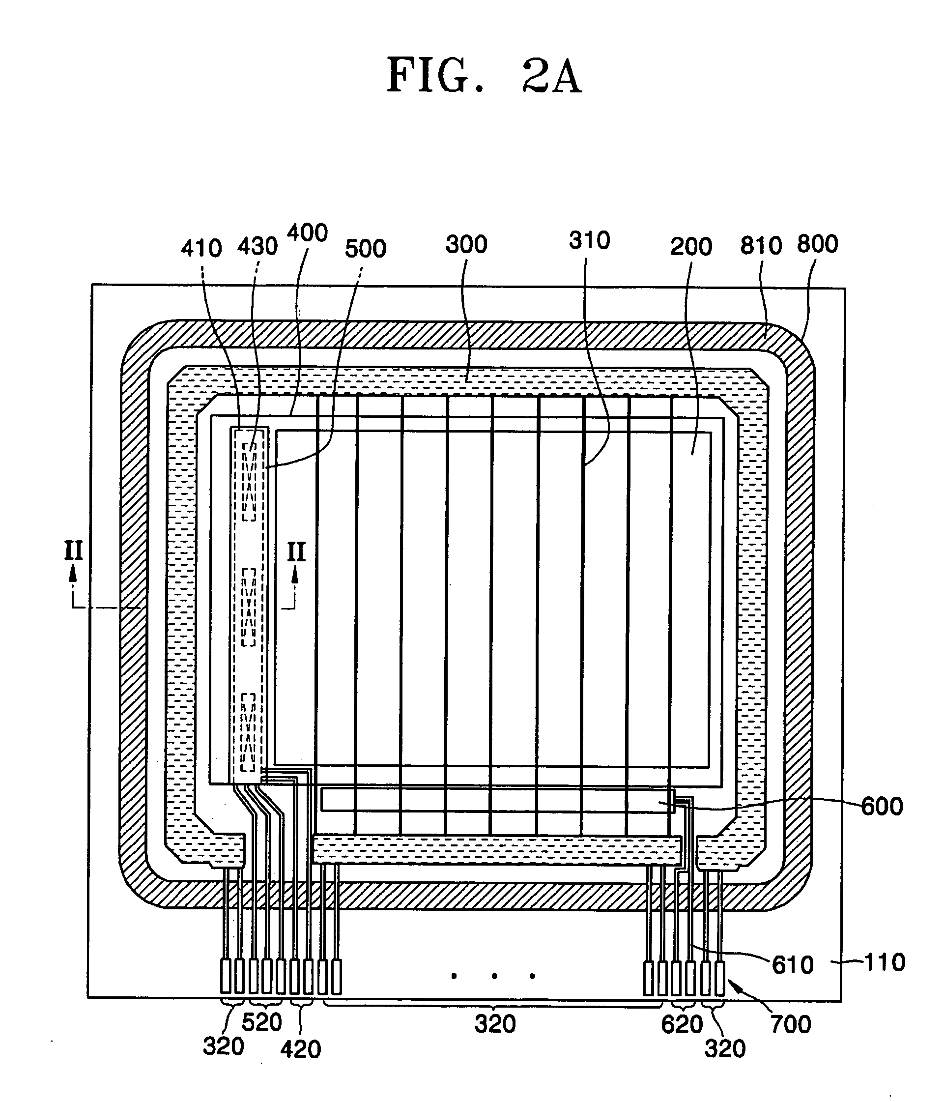
[0032] The present invention will now be described in more detail with reference to the drawings showing examples of specified preferred embodiments. “A layer” can refer to a single layer or to a multi-layer structure. When one layer is described as “on” another, it can be directly on the other, or the two layers may be separated by one or more intervening layers. “Substantial” as used herein, can refer to an amount up to and including the whole amount.

[0033] As shown in FIG. 2A, on one plane of a substrate 110 the following are provided: a display area 200 where a light-emitting device (such as an electroluminescence display device) is disposed, a sealing portion 800 coated on an outer periphery of the display area 200 (for sealing a substrate 110 and an sealing substrate (900 shown in FIG. 2B)), and a terminal region 700 having various terminals. The sealing substrate 900 may be replaced by a sealing thin film layer.

[0034] A structure of the electroluminescence display device fo...


PUM


Abstract

An electroluminescent display device may include a display area formed on one surface of a substrate. It may further include a first electrode layer, a second electrode layer, and an electroluminescent emission layer between the first and second electrode layers. It may also include an electrode power supply line that supplies electrode power to the display area. The electrode power supply line can be located at least partially on an outer periphery of the display area, and may directly contact the second electrode layer. An electrical component may be arranged under the electrode power supply line, and may have one or more conductive layers.

Description

BACKGROUND OF THE INVENTION [0001] This application claims the priority of Korean Patent Application No. 2004-15736, filed Mar. 9, 2004, which is incorporated herein in its entirety by reference. [0002] 1. Field of the Invention [0003] The present invention relates to a flat panel display. More particularly, it relates to an electroluminescence display device that can increase the proportion of display area to substrate area and can reduce nonuniformity in luminance throughout the display area by reducing voltage drop that can occur when supplying voltage to electrodes. [0004] 2. Description of the Related Art [0005] In displaying an image, a variety of display devices are used and, in recent years, there have been numerous kinds of display devices available. Among these display devices, the organic electroluminescent device (a flat emissive-type display device that does not require a separate emission device such as a backlight) has become popular because it enables highly is effic...

Claims


Application Information

Patent Timeline
IPC IPC(8): G09F9/30H01L51/50H01L27/32H05B33/24H05B33/26
CPCH01L27/3276H01L2227/323H01L51/5237H10K59/122H10K59/131H10K50/841H10K59/1201H05B33/26
Inventor KWAK, WON-KYULEE, KWAN-HEE
Owner SAMSUNG DISPLAY CO LTD
Why Eureka
Try Eureka