Microstripline waveguide converter

a converter and microstripline technology, applied in the direction of impedence networks, electrical devices, coupling devices, etc., can solve the problems of deteriorating difficulty in reducing the size of the converter, and inability to reduce unwanted waves, etc., to achieve the enhancement of the electric characteristics of the converter and the reduction of the converter's siz

Inactive Publication Date: 2005-09-15
MITSUBISHI ELECTRIC CORP
View PDF3 Cites 26 Cited by
  • Summary
  • Abstract
  • Description
  • Claims
  • Application Information

AI Technical Summary

Benefits of technology

[0012] Therefore, according to the present invention, a circuit having a band rejection function is provided within the converting portion of a microstripline waveguide converter, thereby enabling the size reduction of the converter.
[0013] Furthermore, according to the present invention, a band rejection function and a microstripline waveguide converter are completely integrated into a single device, thereby enabling the elimination of the working process of connecting the filter with the microstripline waveguide converter.
[0014] In addition, according to the present invention, the need for the interconnection between the filter and the microstripline waveguide converter and the need for the connection thereof using gold wire and gold ribbon, which both easily lead to the reflection of a high frequency signal, are eliminated, thereby enabling the enhancement of the electric characteristics of the converter.

Problems solved by technology

However, the converter using this technique does not have a function of reducing unwanted waves.
Moreover, when the distance between the filter and the microstripline waveguide converter is short, there is a problem that the size reduction of the converter is difficult because of the occurrence of their mutual interference.
Further, because these wire and ribbon easily lead to reflection, there is a problem that the electric characteristics of the converter can be deteriorated if the accuracy of the assembly is not high.

Method used


Image

  • Microstripline waveguide converter
  • Microstripline waveguide converter
  • Microstripline waveguide converter

Examples


first embodiment

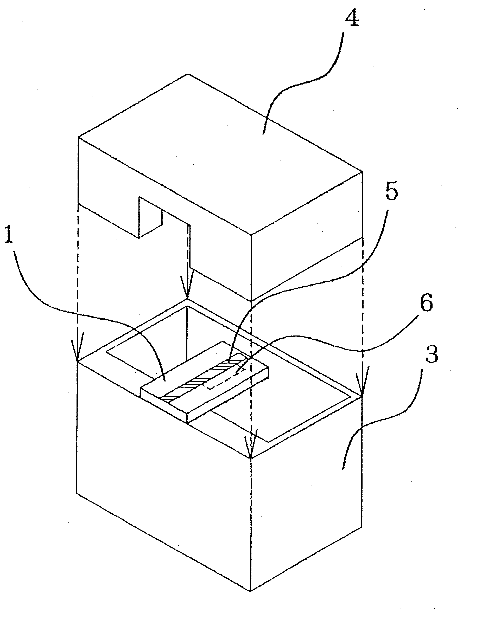
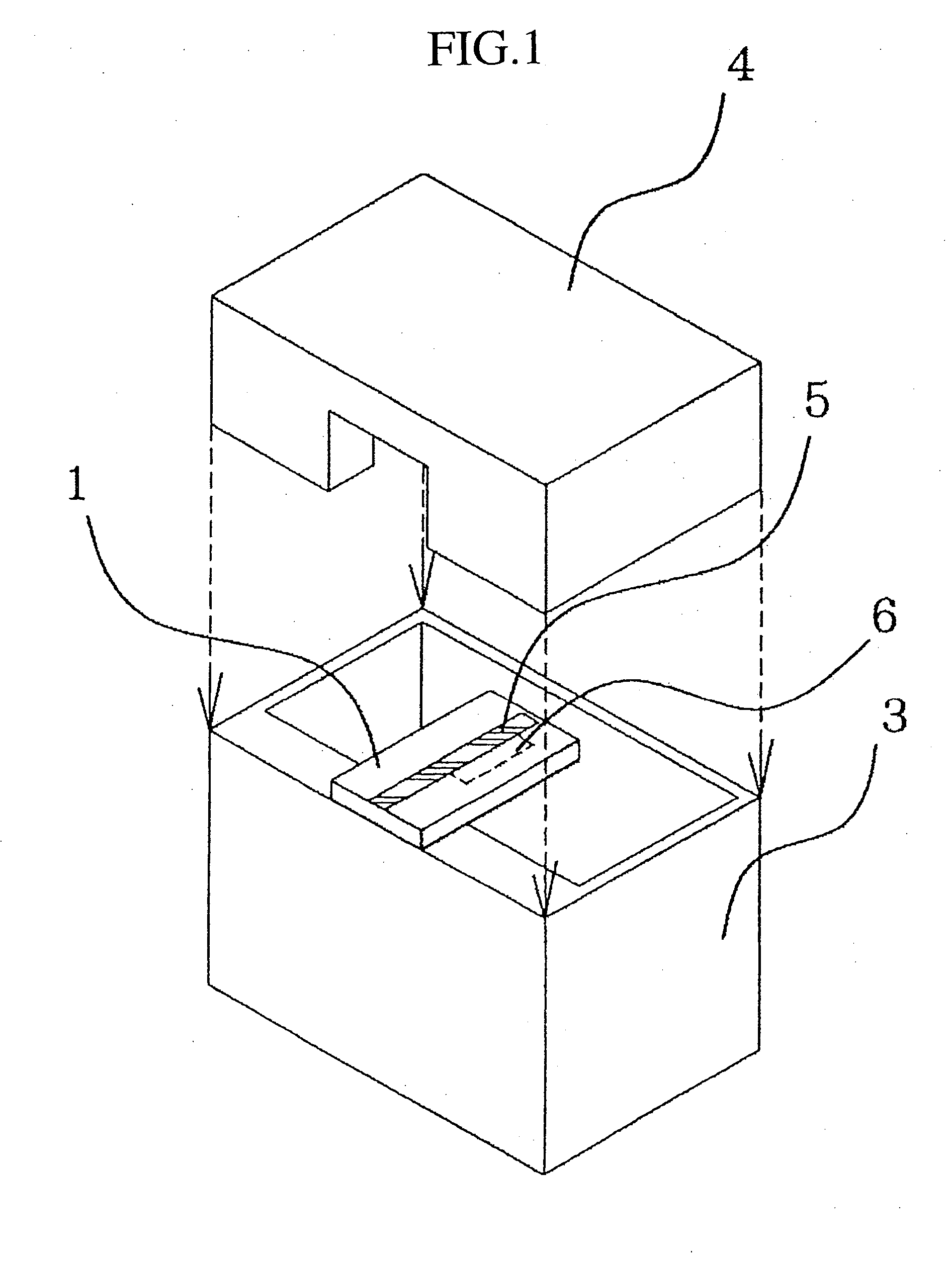
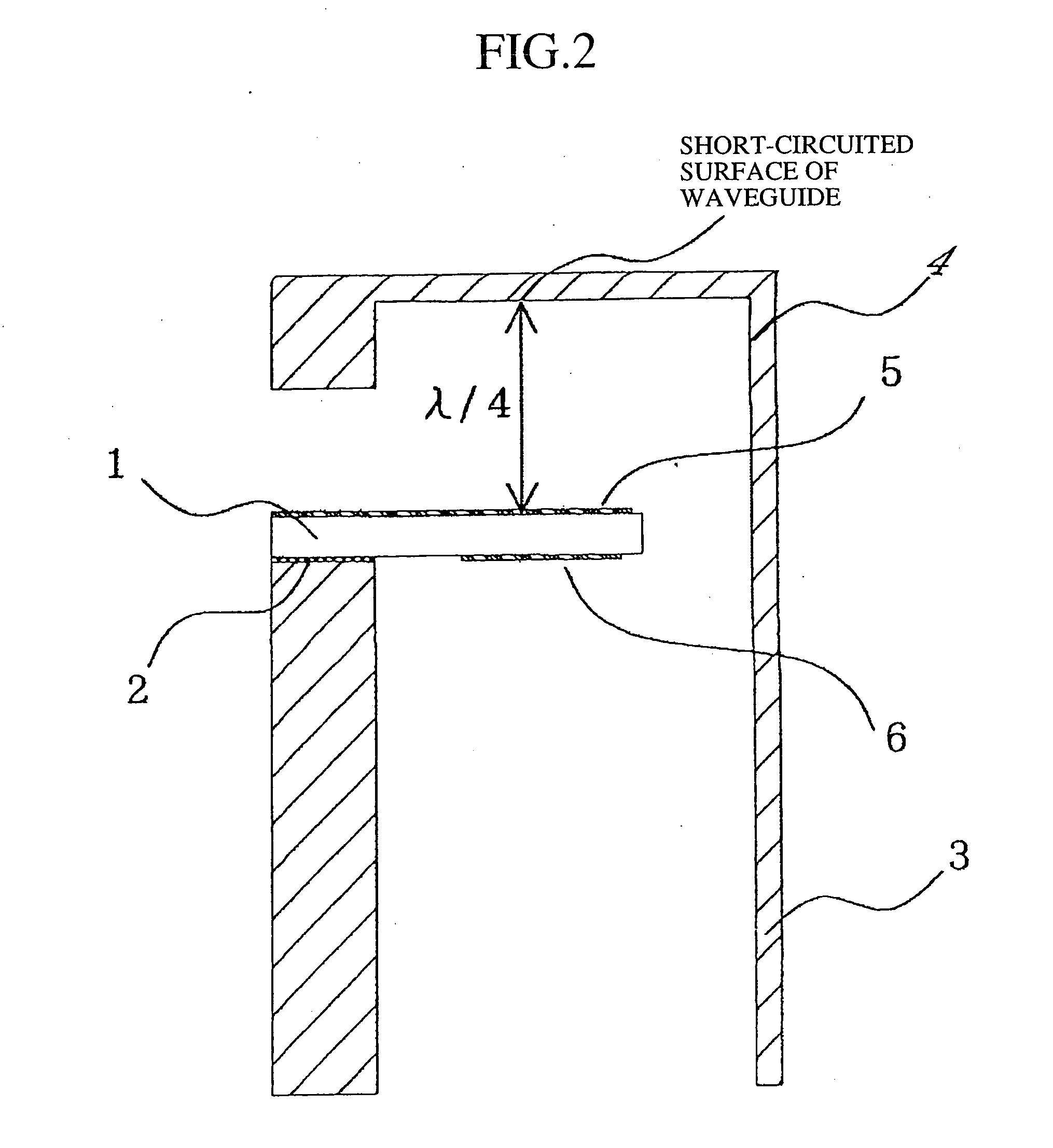
[0037] The configuration of a microstripline waveguide converter according to a first embodiment of the present invention will now be described by reference to FIGS. 1-5.

[0038]FIG. 1 is a perspective view of the configuration of the microstripline waveguide converter according to the first embodiment of the present invention. FIG. 2 is a sectional view of the microstripline waveguide converter shown in FIG. 1. FIG. 3 illustrates a conductor pattern disposed on the top surface of the dielectric substrate shown in FIG. 1 and FIG. 2. FIG. 4 illustrates conductor patterns disposed on the bottom surface of the dielectric substrate.

[0039] In FIGS. 1-4, the reference numeral 1 represents a dielectric substrate, the numeral 2 represents a ground conductor pattern, the numeral 3 represents a waveguide, the numeral 4 represents a short-circuited waveguide block, and the numerals 5 and 6 represent strip conductor patterns formed on the dielectric substrate 1, respectively. In these figures, ...

second embodiment

[0049] The microstripline waveguide converter according to a second embodiment 2 will be described by reference to FIG. 6 and FIG. 7. FIG. 6 is a perspective view of the configuration of a microstripline waveguide converter according to Embodiment 2 of the present invention. FIG. 7 illustrates conductor patterns disposed on the bottom surface of the dielectric substrate shown in FIG. 6.

[0050] According to the second embodiment, the shape of the strip conductor pattern 6, which is disposed on the bottom surface of the dielectric substrate 1, shown in FIG. 6 and FIG. 7, is arranged so as to be of meander-line shape, thereby enabling the band broadening of the rejection band. Moreover, according to the second embodiment, the band one-half wavelength of which is longer than the length of the strip conductor pattern 5, which projects into the waveguide 3, can be reduced.

[0051] Additionally, when the strip conductor pattern 6 has a shape of L character type, T character type, cross type...

third embodiment

[0053] The microstripline waveguide converter according to a third embodiment of the present invention will be described by reference to FIG. 9 and FIG. 10. FIG. 9 is a perspective view of the configuration of a microstripline waveguide converter according to the third embodiment of the present invention. FIG. 10 illustrates conductor patterns disposed on the bottom surface of the dielectric substrate shown in FIG. 9.

[0054] In the third embodiment, a plurality of strip conductor patterns 6 each having a length different from each other are provided on the bottom surface of the dielectric substrate 1 shown in FIG. 9 and FIG. 10, thereby reducing a plurality of unwanted waves. Therefore, according to the third embodiment, similarly as in the first embodiment, the band rejection function can be provided in the inside of the converting portion of the microstripline waveguide converter, and additionally, a plurality of unwanted waves can be reduced.


PUM


Abstract

In the inside of the converting portion of a microstripline waveguide converter, on the backside surface of a dielectric substrate, which constitutes, for example, a “stripline antenna,” a strip conductor pattern, which serves as a half-wavelength strip resonator, is disposed, to thereby add a band rejection function to the converter. The size of the converter is thereby reduced.

Description

BACKGROUND OF THE INVENTION [0001] 1. Field of the Invention [0002] The present invention relates to a microstripline waveguide converter used mainly in a microwave band and a millimeter wave band. [0003] 2. Description of Related Art [0004] As a conventional microstripline waveguide converter, for example, JP-A-2000-244212 discloses a converter in which a microstripline is extended to form a stripline antenna, the antenna is inserted in the opening of a waveguide, and one of the surfaces of the waveguide is short-circuited at the position that is approximately one quarter of the guide wavelength from the pattern of a strip conductor. According to this technique, because the magnetic field in the waveguide becomes the maximum at the position at which the strip conductor pattern is inserted, the propagation mode of the microstripline and that of the waveguide well couple with each other, and the high frequency signal that has been propagated through the microstripline can be propagat...

Claims


Application Information

Patent Timeline
Patent Type & Authority Applications(United States)
IPC IPC(8): H01P5/107
CPCH01P5/107
Inventor TAKEDA, HIDEJIASAO, HIDEKITSUZUKI, HIDEKIKATAYAMA, AKIKO
Owner MITSUBISHI ELECTRIC CORP
Why Eureka
Try Eureka