Lumped-element low-pass filter in multi-layered substrate

a low-pass filter and multi-layer technology, applied in the field of low-pass filter performance of low-pass filter, can solve the problems of large number of circuit elements, and inability to meet the requirements of high-frequency circuit design, so as to improve the rejection effect, reduce the cost of manufacturing, and save circuit area

Inactive Publication Date: 2005-09-15
CHI MEI COMM SYST INC
View PDF6 Cites 23 Cited by
  • Summary
  • Abstract
  • Description
  • Claims
  • Application Information

AI Technical Summary

Benefits of technology

[0009] It is an advantage of the claimed invention that utilization of the mutual inductance improves rejection in the stop-band of the conventional elliptic-type low-pass filter without adding additional circuit elements. In the claimed invention, a shar...

Problems solved by technology

Performance of low-pass filter is characterized by insertion loss in the passband and rejection in the stopband.
However, filter of higher order requires more elements in filter designs, which leads to a larger circuit size and more insertion loss.
Low...

Method used


Image

  • Lumped-element low-pass filter in multi-layered substrate
  • Lumped-element low-pass filter in multi-layered substrate
  • Lumped-element low-pass filter in multi-layered substrate

Examples


first embodiment

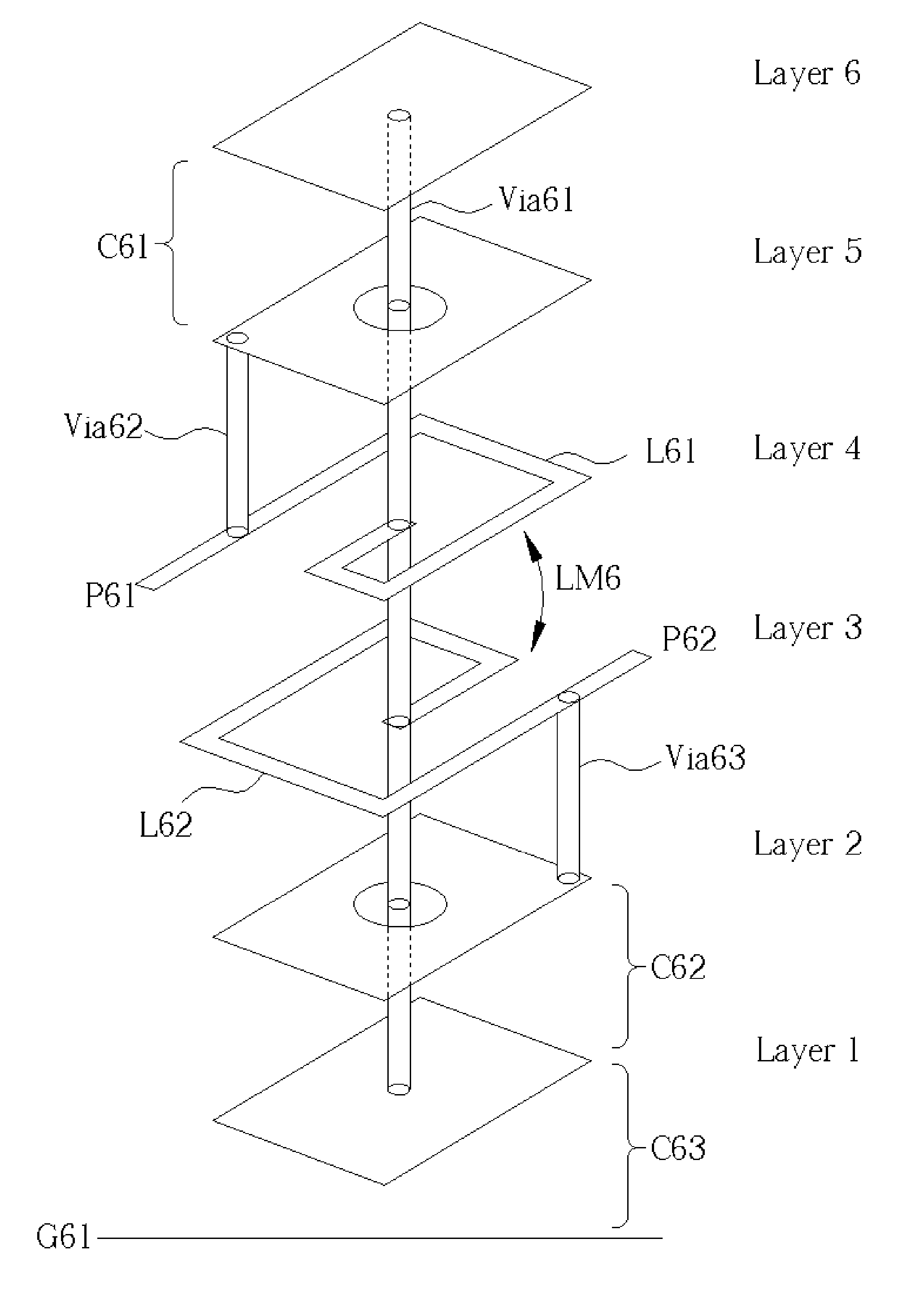
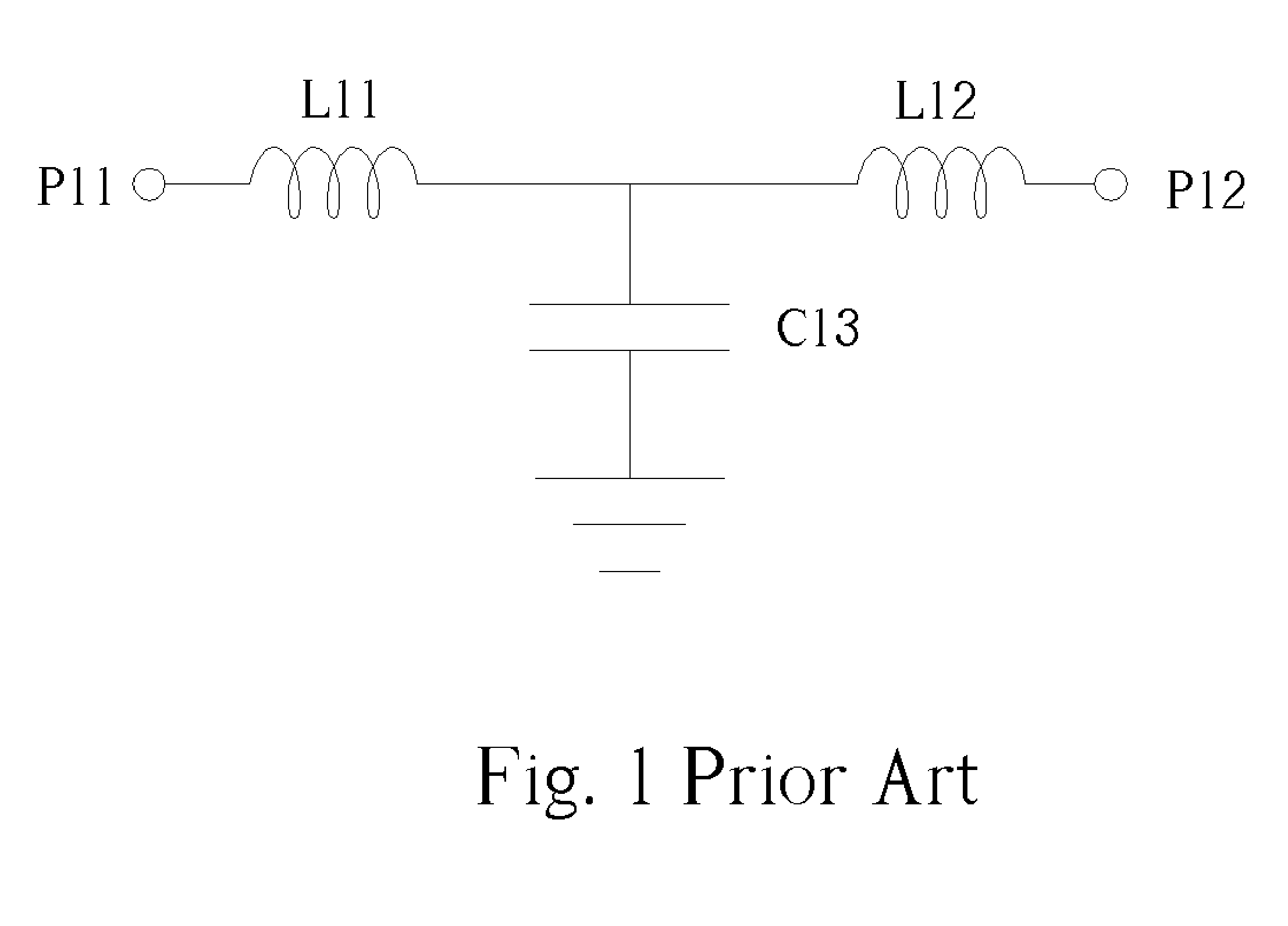
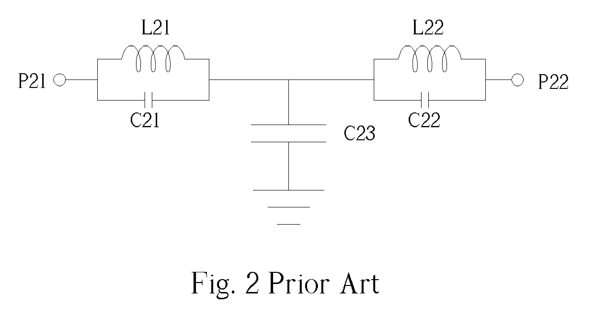
[0023] It is known that the mutual inductance relates to the distance and geometrical relations between the two inductors. Therefore, it is very applicable to implement the present invention in a 3-dimensional structure such as a multi-layered substrate. Based on the aforementioned circuit model shown in FIG. 4, a novel lumped-element low-pass filter with good stopband rejection may be realized in a very small area. Please refer to FIG. 6. FIG. 6 shows the present invention realized in a multi-layered substrate with a bottom ground plane G61. The filter includes inductors L61 and L62, capacitors C61, C62, and C63, and vias Via61, Via62, and Via63 penetrating the substrate and connecting different layers. Inductors L61 and L62 are realized with rectangular conductive spirals on layer 4 and layer 3 respectively. Note that the orientations of inductors L61 and L62 are different, such that a negative mutual inductance LM6 is established between inductors L61 and L62 with this arrangemen...

second embodiment

[0024]FIG. 8 shows the present invention realized in a multi-layered substrate with both a top ground plane G82 and a bottom ground plane G81. FIG. 8 illustrates inductors L81 and L82, capacitors C81, C82, and C83, and vias Via81, Via82, and Via83 penetrating the substrate and connecting different layers. The inductors L81 and L82 are realized by circular conductive spirals on layer 4 and layer 3 respectively. Note that the orientations of the inductors L81 and L82 are different. A negative mutual inductance LM8 is established between the inductors L81 and L82 with this arrangement, and it may achieve a designed value by appropriately adjusting the shapes of L81 and L82, or by selection of the distance between layer 3 and layer 4. The inductor L82 is electrically connected to the inductor L81 in series through the via Via81 penetrating the substrate. The capacitor C81 comprises two plates formed on layer 5 and layer 6. The plate formed on layer 5 is connected to one end of the induc...

third embodiment

[0025] Please refer to FIG. 9. FIG. 9 is the present invention realized in a multi-layered substrate with a bottom ground plane G91. FIG. 9 illustrates inductors L91 and L92, capacitors C91, C92, and C93, and vias Via91, Via92, and Via93 penetrating the substrate and connecting different layers. Inductors L91 and L92 are realized by rectangular conductive spirals on layer 4 and layer 3 respectively. The orientations of inductors L91 and L92 are different so that a negative mutual inductance LM9 is established between inductors L91 and L92 with this arrangement. The inductor L92 is electrically connected to the inductor L91 in series through the via Via91. The capacitor C91 comprises two plates formed on layer 5 and layer 6. The plate formed on layer 6 is connected to one end of the inductor L91 through the via Via92 and the plate formed on layer 5 is connected to another end of the inductor L91 through the via Via91. That is, the capacitor C91 is shunt-connected to the inductor L91 ...


PUM


Abstract

A lumped-element low-pass filter is formed in a multi-layered substrate. A negative mutual inductance between two inductors is adjusted to a designed value and utilized to improve the rejection in the stopband of the low-pass filter. The two inductors are spiral in shape and the orientations of the first inductor and the second inductor are of opposite sense such that a mutual inductance between the first inductor and the second inductor is negative and equals a designed value. A first capacitor and a second capacitor are shunt-connected to the first and the second inductor respectively to form the elliptic-type filter. A third capacitor is electrically connected to ground at its first end, and electrically connected to the end of the second inductor at which the second inductor in electrically connected to the first inductor in series at its second end.

Description

BACKGROUND OF INVENTION [0001] 1. Field of the Invention [0002] The present invention relates to a lumped-element low-pass filter, and more particularly, to a lumped-element low-pass filter realized in a multi-layered substrate. [0003] 2. Description of the Prior Art [0004] Low-pass filters are widely used as building blocks in circuit designs. They are usually used to filter out unwanted spurious responses and harmonics of higher frequencies. Performance of low-pass filter is characterized by insertion loss in the passband and rejection in the stopband. The level of rejection in the stopband is mainly determined by the order of the filter. The higher the order of the filter, the better the rejection in the stopband. However, filter of higher order requires more elements in filter designs, which leads to a larger circuit size and more insertion loss. Shown in FIG. 1 is a prototype circuit of a conventional third order low-pass filter. P11 and P12 are two ports of the filter. L11 and...

Claims


Application Information

Patent Timeline
IPC IPC(8): H03H7/01H05K1/00H05K1/02H05K1/16
CPCH03H7/0115H03H7/1766H03H2001/0085H05K1/0237H03H7/09H05K1/162H05K1/165H05K2201/09672H05K1/0298
Inventor LIN, YO-SHENLI, KO-MAI
Owner CHI MEI COMM SYST INC
Why Eureka
Try Eureka