Method for variability constraints in design of integrated circuits especially digital circuits which includes timing closure upon placement and routing of digital circuit or network

Inactive Publication Date: 2005-09-22
PANASONIC CORP
View PDF7 Cites 141 Cited by
  • Summary
  • Abstract
  • Description
  • Claims
  • Application Information

AI Technical Summary

Benefits of technology

[0021] As has been described, according to the present invention, in each standard cell, the surface area, gate length or perimeter of a gate electrode of each of dummy transistors belonging to a standard cell and the area of each of substrate contacts belonging to the standard cell are adjusted, so that among standard cells, a difference in the total surface area or total perimeter of respective gate electrodes of all transistors belonging to a standard cell, or a difference in the total area or

Problems solved by technology

For example, when a circuit pattern of a reticle is exposed to light and transferred to a photo resist applied onto a semiconductor wafer by irradiating light to the reticle of a semiconductor integrated circuit using a photolithography device, a predetermined device length of a fabricated circuit device can not be achieved but the de

Method used


Image

  • Method for variability constraints in design of integrated circuits especially digital circuits which includes timing closure upon placement and routing of digital circuit or network
  • Method for variability constraints in design of integrated circuits especially digital circuits which includes timing closure upon placement and routing of digital circuit or network
  • Method for variability constraints in design of integrated circuits especially digital circuits which includes timing closure upon placement and routing of digital circuit or network

Examples


embodiment 1

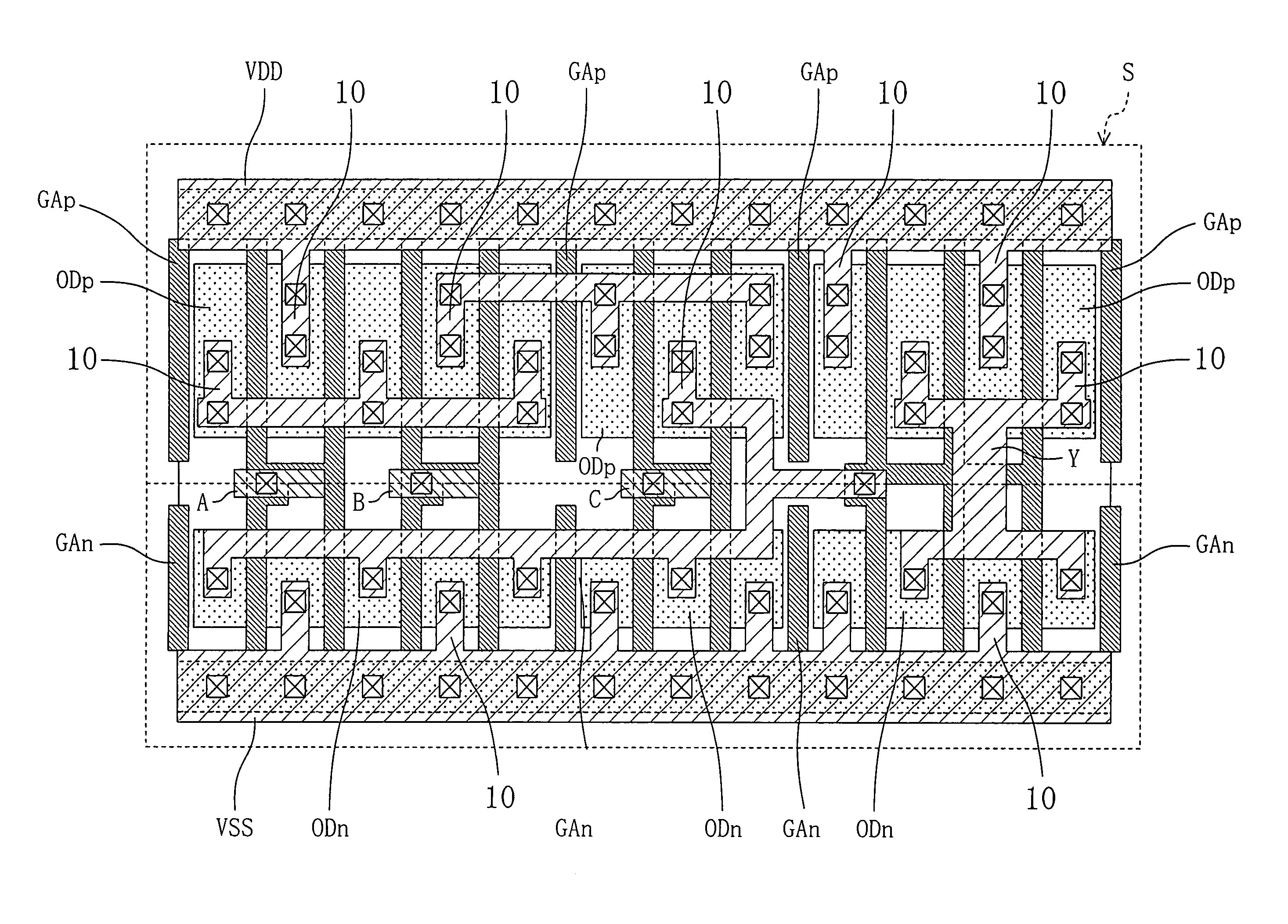
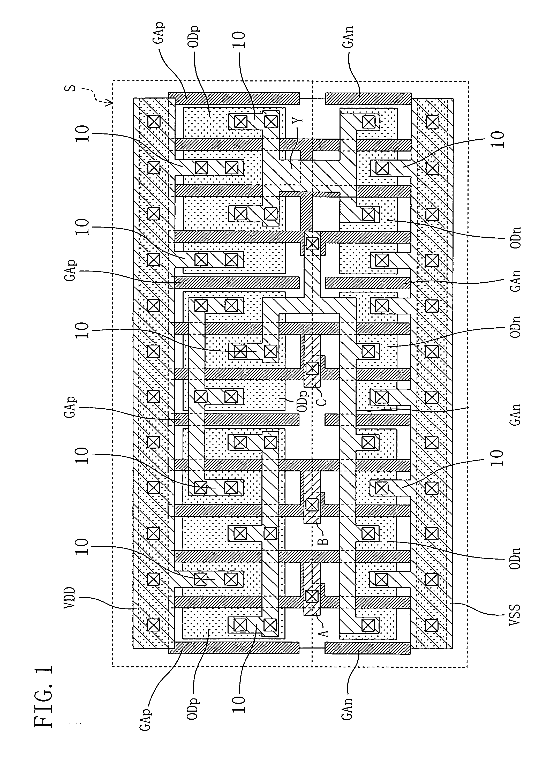
[0033]FIG. 1 is a view illustrating a layout structure of a standard cell according to an embodiment of the present invention. In a standard cell S of FIG. 1, VDD denotes a power source line, VSS denotes a ground line, 10 denotes a gate electrode, and ODp and ODn denotes diffusion regions. A plurality of polysilicon gate electrodes 10 (24 gate electrodes in FIG. 1) are arranged above diffusion regions ODp and ODn, so that 12 p-type and n-type MOSFET transistors (which will be hereafter referred to as “active transistors”) to be normally used are formed.

[0034] Furthermore, in the standard cell S, GAp and GAn are of a polysilicon gate electrode connected to a source supply line VDD or a ground line VSS. Each of the polysilicon gate electrodes is located at a side of an associated one of the diffusion regions ODp and ODn and does not intersect with the associated one of the diffusion regions ODp and ODn. Thus, each of the gate electrodes GAp and GAn forms part of a p-type or n-type MO...

embodiment 2

[0041] Next, Embodiment 2 of the present invention will be described.

[0042] In Embodiment 1, the surface area of each of the dummy gate electrodes GAp and GAn are adjusted to reduce influences on transistor characteristics due to the layout dependency. In contrast, according to this embodiment, to reduce the layout pattern dependency, a perimeter of each of the dummy gate electrodes GAp and GAn is adjusted thereby reducing influences on transistor characteristics.

[0043]FIG. 4 is a view illustrating gate electrode part taken out of the layout structure of a standard cell S. The total perimeter of respective gate electrodes of all transistors belonging to a cell differs depending to the type of the cell. Then, in FIG. 4, the respective lengths Lp and Ln of dummy gate electrodes GAp and GAn are adjusted to reduce a difference in the total perimeter of respective gate electrodes of all transistors of the cell among cells of different types, thereby reducing influences on transistor ch...

embodiment 3

[0046] Subsequently, Embodiment 3 of the present invention will be described with reference to FIG. 5. In this embodiment, a predetermined semiconductor integrated circuit is formed using a plurality of standard cells according to the present invention.

[0047] In FIG. 5, three standard cells SA, SB, and SC are used. For the cells SA, SB, and SC, cells of Embodiment 1 or Embodiment 2 in which the surface area and perimeter of dummy gate electrodes are adjusted are used. In FIG. 5, the cells SA and SC located on the left and the right, respectively, are the same type of cells and the cell SB located in the center is a cell of a different type. In each of the cells, as has been described, the dummy gate electrodes GAp and GAn are provided at left and right end sections. The lengths of the dummy gate electrodes GAp and GAn are adjusted so that a difference between the cell SA and the cell SB and a difference between the cell SC and the cell SB in the total surface area or total perimete...


PUM


Abstract

In a standard cell, dummy transistors have p-type and n-type dummy gate electrodes. The dummy transistors are in an OFF state all the time. The gate length of each of the dummy gate electrodes is extended over an end portion of a diffusion region toward the inside of the standard cell. Thus, the total surface area and the total perimeter of respective gate electrodes of all transistors provided in the standard cell are increased. As a result, for example, even though shapes of gate electrodes of transistors vary between the standard cell and each of other standard cells, transistor characteristics are substantially equal among the standard cells. Therefore, variations in delays of signals generated between the standard cells can be suppressed.

Description

CROSS REFERENCE TO RELATED APPLICATIONS [0001] This non-provisional application claims priority under 35 U.S.C. § 119(a) on Patent Application No. 2004-080618 filed in Japan on Mar. 19, 2004, the entire contents of which are hereby incorporated by reference. BACKGROUND OF THE INVENTION [0002] The present invention relates to a standard cell design method and a semiconductor integrated circuit fabricated by placement and routing using standard cells designed by the design method, and more preferably relates to a cell design method and a semiconductor integrated circuit which suppresses delay variations depending on a layout pattern. [0003] In recent years, there has been rapid progress in reduction in size and improvement of functions for semiconductor integrated circuits. With the progress, the device length of semiconductor integrated circuits has been reduced for the purpose of improving performances of transistors. [0004] In process steps for fabricating a semiconductor integrate...

Claims


Application Information

Patent Timeline
IPC IPC(8): H01L21/822H01L21/82H01L27/02H01L27/04H01L27/10H01L27/118
CPCH01L27/11807H01L27/0207
Inventor SUMIKAWA, TAKASHIYAMASHITA, KYOJIMOTOJIMA, DAI
Owner PANASONIC CORP
Why Eureka
Try Eureka