Optoelectronic semiconductor component

a technology of optoelectronic semiconductors and semiconductor components, which is applied in the direction of semiconductor devices, semiconductor/solid-state device details, electrical apparatus, etc., can solve the problems of limiting use, the curvature precision of the curved surface of the optical reflection is increased, and the disadvantages of improving, so as to reduce the total strain, enhance the illumination efficiency of the semiconductor chip, and reduce the total strain

Inactive Publication Date: 2005-09-22
LITE ON TECH CORP
View PDF6 Cites 52 Cited by
  • Summary
  • Abstract
  • Description
  • Claims
  • Application Information

AI Technical Summary

Benefits of technology

[0010] The present invention provides an optoelectronic semiconductor component that has an improved encapsulation body for resisting the influence of outer forces and further lowering total strain, in particular the deformation of an optical reflection curved-surface. Therefore, the curvature precision of the optical reflection curved-surface is increased, the illumination efficiency of the semiconductor chip is enhanced, and emission is uniform.
[0011] The present invention further provides an optoelectronic semiconductor component that fixes the chip accurately, so that the semiconductor chip emits uniformly and increases the combinative ability of the chip with the chip carrier of lead frame, therefore enhancing the reliability of the optoelectronic semiconductor component.
[0012] The present invention provides an optoelectronic semiconductor component, which comprises a lead frame, at least one radiation-emitting / or radiation-receiving semiconductor chip, an encapsulation body, an optical window part, and a pair of outside connecting parts. The lead frame has a chip carrier and an independent link-part. The chip carrier is formed with a central position mark thereon and defined as an inner electrical contact. The independent link-part is another inner electrical contact. The semiconductor chip is secured on the chip carrier and is electrically connected with the chip carrier and the independent link-part via leads, respectively. The encapsulation body is formed with an axial-symmetrical arc section, which is centered on the semiconductor chip. An inner surface of the encapsulation body encircles a part of the chip carrier and the independent link-part to define an annular ellipsoid. The optical window part is formed in a concave portion of the annular ellipsoid and is filled with a material for transforming optical characteristic of emitted / or received light from the semiconductor chip. The pair of outside connecting parts respectively extends from the chip carrier and the independent link-part, and is exposed by the encapsulation body as outer contacts; thereby resisting the influence of external force, reducing total strain, and increasing the curvature precision of the optical-reflecting curved surface to enhance the emitting efficiency of the semiconductor chip and solve the light loss of such kind illumination structure.

Problems solved by technology

Such a structure cannot make the light direction parallel to the PCB, thus limiting the use thereof.
Therefore, the optoelectronic semiconductor module of the prior art still has some inconvenience and disadvantages to be improved.

Method used


Image

  • Optoelectronic semiconductor component
  • Optoelectronic semiconductor component
  • Optoelectronic semiconductor component

Examples


second embodiment

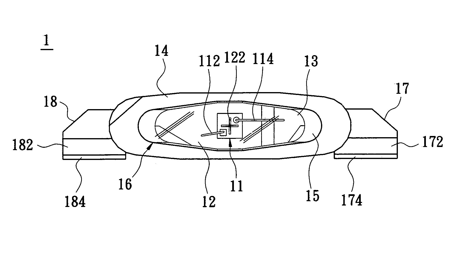
[0035]FIG. 11 illustrates a front view of the optoelectronic semiconductor component of second embodiment according to the present invention. The optoelectronic semiconductor component la can be mounted with more than one semiconductor chips 11, 11a with different function. For example, mounting with two LED semiconductor chips to meet the requirement of better illumination and enhance the reliability of the LED semiconductor chips, or mounting with another one diode-protective chip to protect the semiconductor chip 11 from excessive current, such as a Zener diode. The Zener diode can adjust working voltage and has function of stabilizing circuit. The optoelectronic semiconductor component 1 a is formed with two central position marks 122, 123 on the chip carrier 12 to orientate the semiconductor chips 11, 11a. The semiconductor chips 11, 11a are parallel or series connection via the leads 112, 113, 114.

[0036]FIG. 12 illustrates a side view of the optoelectronic semiconductor compon...

third embodiment

[0037]FIG. 13, 14 illustrate a front view of the optoelectronic semiconductor component of third embodiment according to the present invention, and a side view of the optoelectronic semiconductor component assembled on a PCB. The fixing portions 17a, 18a of the optoelectronic semiconductor component 1a are formed into slab-shape that are extending outside the encapsulation body 14 and perpendicular to the emission direction. The optoelectronic semiconductor component la therefore can be soldered on PCB 2 vertically.

[0038] The geometric structure of the outer electric contacts of the present invention can reduce the contact resist and increase the heat-conductive factor to enhance the emitting efficiency of the semiconductor chip and solve the light loss of such kind illumination structure.

[0039] A summary of the characteristics and advantages of the optoelectronic semiconductor component is given as follows.

[0040] The encapsulation body 14 of the present invention is an arc with a...


PUM


Abstract

An optoelectronic semiconductor component applies to a surface mount component of an optoelectronic semiconductor. The optoelectronic semiconductor component has one or more semiconductor chip secured on a chip carrier. The chip carrier is a part of a lead frame, and another part of the lead frame is formed with an independent connection part as a contact of the semiconductor chip. An encapsulation body centers on the semiconductor chip and encircles part of the chip carrier and the independent connection part to form an annular ellipsoid for reflecting or receiving radiation of the semiconductor chip. The encapsulation body has a recess and a window part filling the recess. The window part is composed of materials for transforming the optical characteristics of the semiconductor chip. Part of the chip carrier and the independent connection part extend out the encapsulation body to form outside contacts as a SMT component.

Description

BACKGROUND OF THE INVENTION [0001] 1. Field of the Invention [0002] The present invention relates to an optoelectronic semiconductor component, and particularly to an SMT-type (surface mounted technology-type) optoelectronic semiconductor component for illumination that can be applied as a backlight source or a light interceptor. [0003] 2. Description of the Prior Art [0004] LED (Light Emitting Diode) is a kind of solid-state illuminant that is small-scale and has high lighting efficiency. It has a long lifespan and high stability. LED is adopted as various types of light sources, such as a light source for a monitor, a backlight board, a traffic signal, emergency exits, or decorative illumination, because LED is a kind of semiconductor component. [0005] Similar optoelectronic semiconductor modules have been disclosed, as in U.S. Pat. No. D478877 (shown in FIGS. 1 and 2) which has been issued on Aug. 26, 2003 and R.O.C. patent number 315528 (shown in FIGS. 3 and 4) which has been is...

Claims


Application Information

Patent Timeline
Patent Type & Authority Applications(United States)
IPC IPC(8): H01L23/02H01L25/16H01L33/48H01L33/50H01L33/54H01L33/60H01L33/62
CPCH01L25/167H01L33/486H01L33/54H01L33/60H01L2224/48091H01L33/62H01L2924/00014
Inventor SU, HUNG-YUANWU, CHUNG-CHANSU, SHU-YUN
Owner LITE ON TECH CORP
Why Eureka
Try Eureka