Methods and systems for determining one or more properties of a specimen

a technology of specimens and properties, applied in the field of methods and systems for determining one or more properties of specimens, can solve the problems of inability to achieve continuous illumination, disadvantage, and adjustment of photon flux at each wavelength, and achieve the effect of constant illumination flux

Active Publication Date: 2005-09-22
KLA TENCOR TECH CORP
View PDF13 Cites 24 Cited by
  • Summary
  • Abstract
  • Description
  • Claims
  • Application Information

AI Technical Summary

Problems solved by technology

For example, the systems described in U.S. Pat. No. 4,333,051 to Goodman have the disadvantage that the photon flux has to be adjusted at each wavelength to achieve the same SPV signal.
Even using a servo to achieve this adjustment, there is a throughput disadvantage due to the time required to measure the SPV signal and adjust the flux accordingly.
The systems described in U.S. Pat. No. 5,025,145 to Lagowski and U.S. Pat. No. 5,663,657 to Lagowski et al. have the disadvantage that the wavelengths are sent to the wafer sequentially.
This configuration results in a throughput loss, as the same measurement site has to be sequentially illuminated with each wavelength.
These changes alter the SPV signal value and thereby create errors in diffusion length measurements.
However, these systems have the disadvantage that the wavelengths are modulated at two different frequencies.
Inspection is performed to detect defects such as electrical defects and / or any number of other types of defects, which may have been inadvertently formed on the wafer, some of which may adversely affect the performance of integrated circuits that are eventually formed on the wafer.
However, if there is a defect present, the number of dark and bright features within the generated image will not match expected results.
Performing inspection in a vacuum environment is more expensive and slower than performing inspection in an ambient environment.
Therefore, the data that can be generated by such inspection methods and systems may be somewhat limited, particularly for use in identification of defect types (i.e., classification).

Method used


Image

  • Methods and systems for determining one or more properties of a specimen
  • Methods and systems for determining one or more properties of a specimen
  • Methods and systems for determining one or more properties of a specimen

Examples


Embodiment Construction

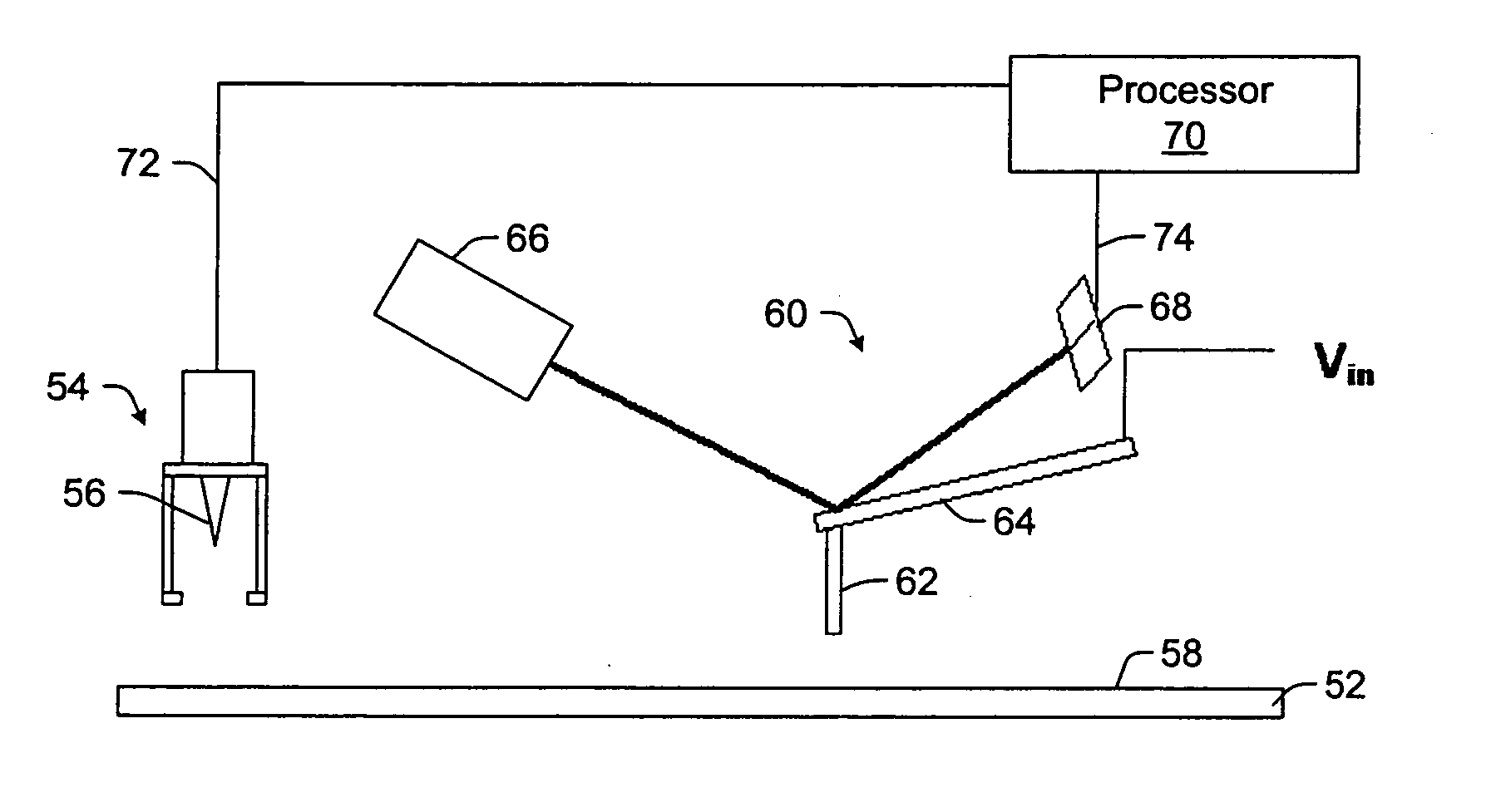
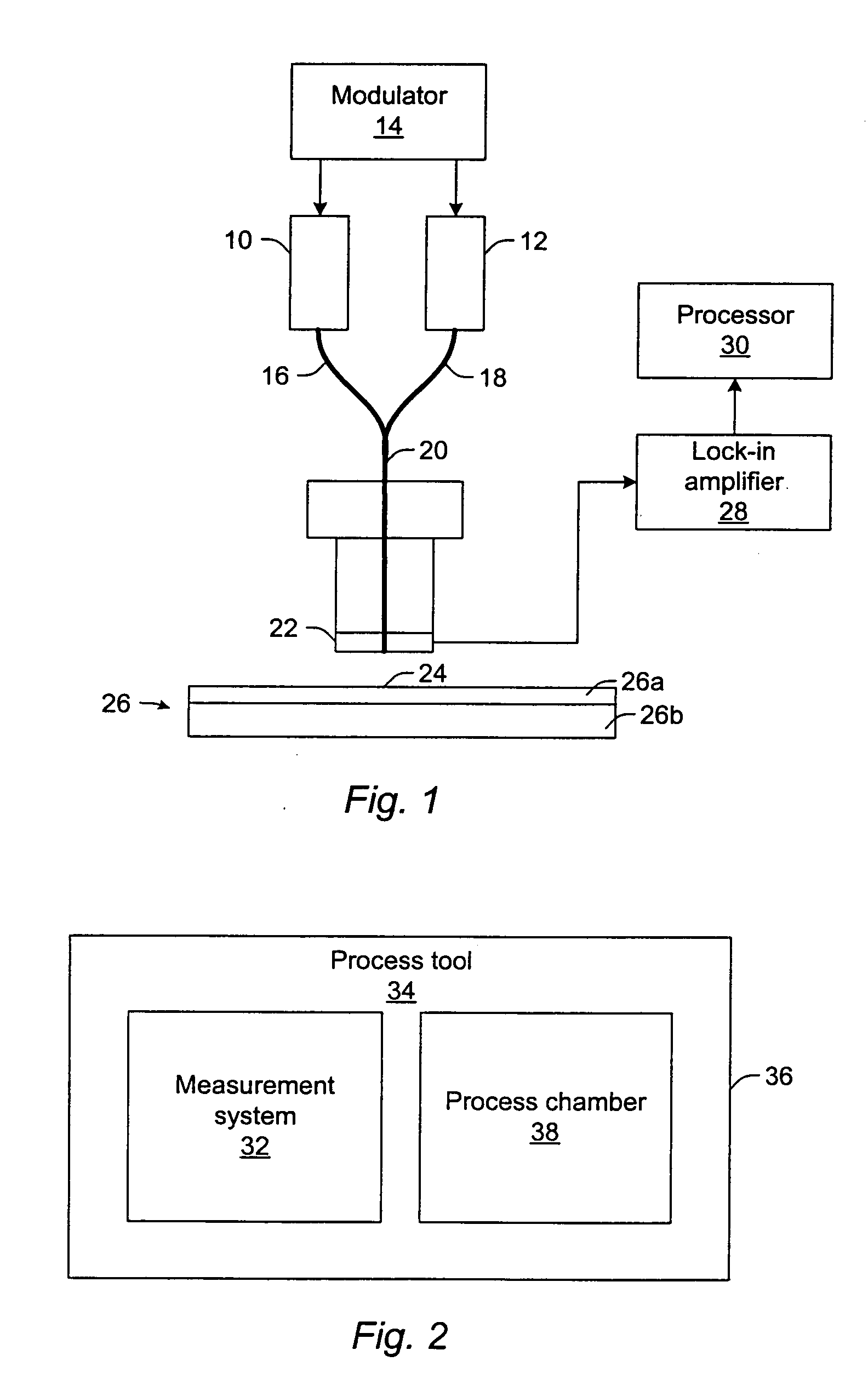
[0037] As used herein, a “specimen” is generally defined as a wafer or any other specimen known in the art. The term “wafer” generally refers to a substrate formed of a semiconductor or a non-semiconductor material. Examples of such a semiconductor or non-semiconductor material include, but are not limited to, monocrystalline silicon, gallium arsenide, and indium phosphide. Such substrates may be commonly found and / or processed in semiconductor fabrication facilities.

[0038] A wafer may include only a substrate. Such a wafer is commonly referred to as a “virgin wafer.” Alternatively, a wafer may include one or more layers formed upon a semiconductor substrate. For example, such layers may include, but are not limited to, a resist, a dielectric material, and a conductive material. A resist may include a resist that may be patterned by an optical lithography technique, an e-beam lithography technique, or an X-ray lithography technique. Examples of a dielectric material include, but ar...


PUM


Abstract

Various methods and systems for determining one or more properties of a specimen are provided. One system for determining a property of a specimen is configured to illuminate a specimen with different wavelengths of light substantially simultaneously. The different wavelengths of light are modulated at substantially the same frequency. The system is also configured to perform at least two measurements on the specimen. A minority carrier diffusion length of the specimen may be determined from the measurements and absorption coefficients of the specimen at the different wavelengths. Another system for detecting defects on a specimen is configured to deposit a charge at multiple locations on an upper surface of the specimen. This system is also configured to measure a vibration of a probe at the multiple locations. Defects may be detected on the specimen using a two-dimensional map of the specimen generated from the measured surface voltages.

Description

PRIORITY CLAIM [0001] This application claims priority to U.S. Provisional Application No. 60 / 555,172 entitled “Methods and Systems for Determining One or More Properties of a Specimen,” filed Mar. 22, 2004, which is incorporated by reference as if fully set forth herein.BACKGROUND OF THE INVENTION [0002] 1. Field of the Invention [0003] The present invention generally relates to methods and systems for determining one or more properties of a specimen. Certain embodiments relate to methods and systems for determining a minority carrier diffusion length and contamination levels of a specimen. Other embodiments relate to methods and systems for detecting defects on a specimen. [0004] 2. Description of the Related Art [0005] Methods and systems are currently available for the measurement of minority carrier lifetimes in semiconductor wafers. The minority carrier lifetimes of semiconductor wafers is of interest to semiconductor manufacturers since the minority carrier lifetimes indicate...

Claims


Application Information

Patent Timeline
Patent Type & Authority Applications(United States)
IPC IPC(8): H01L21/66G01R31/26G01R31/311
CPCG01R31/311G01R31/2648
Inventor SHI, JIANOURZEPIELA, JEFFREYPEI, SHIYOUXU, ZHIWEIALEXANDER, JOHN
Owner KLA TENCOR TECH CORP
Why Eureka
Try Eureka