Method to increase coupling ratio of source to floating gate in split-gate flash

a split-gate flash and source technology, applied in semiconductor devices, digital storage, instruments, etc., can solve the problems of punch-through and junction breakdown, additional variation in cell performance, and known problems, and achieve the effect of increasing the coupling ratio

Inactive Publication Date: 2005-09-22
TAIWAN SEMICON MFG CO LTD
View PDF13 Cites 48 Cited by
  • Summary
  • Abstract
  • Description
  • Claims
  • Application Information

AI Technical Summary

Benefits of technology

[0016] It is therefore an object of this invention to provide a method of forming a split-gate flash memory having an increased coupling ratio between source and the floating gate.

Problems solved by technology

However, trying to increase coupling ratio by increasing the source implant lateral diffusion causes the well-known problems of punch-through and junction breakdown.
Furthermore, the uncertainty in the final position of the n+ regions causes variations in the series resistance of the bit lines connected to those regions, and hence additional variation in the cell performance.

Method used


Image

  • Method to increase coupling ratio of source to floating gate in split-gate flash
  • Method to increase coupling ratio of source to floating gate in split-gate flash
  • Method to increase coupling ratio of source to floating gate in split-gate flash

Examples


Embodiment Construction

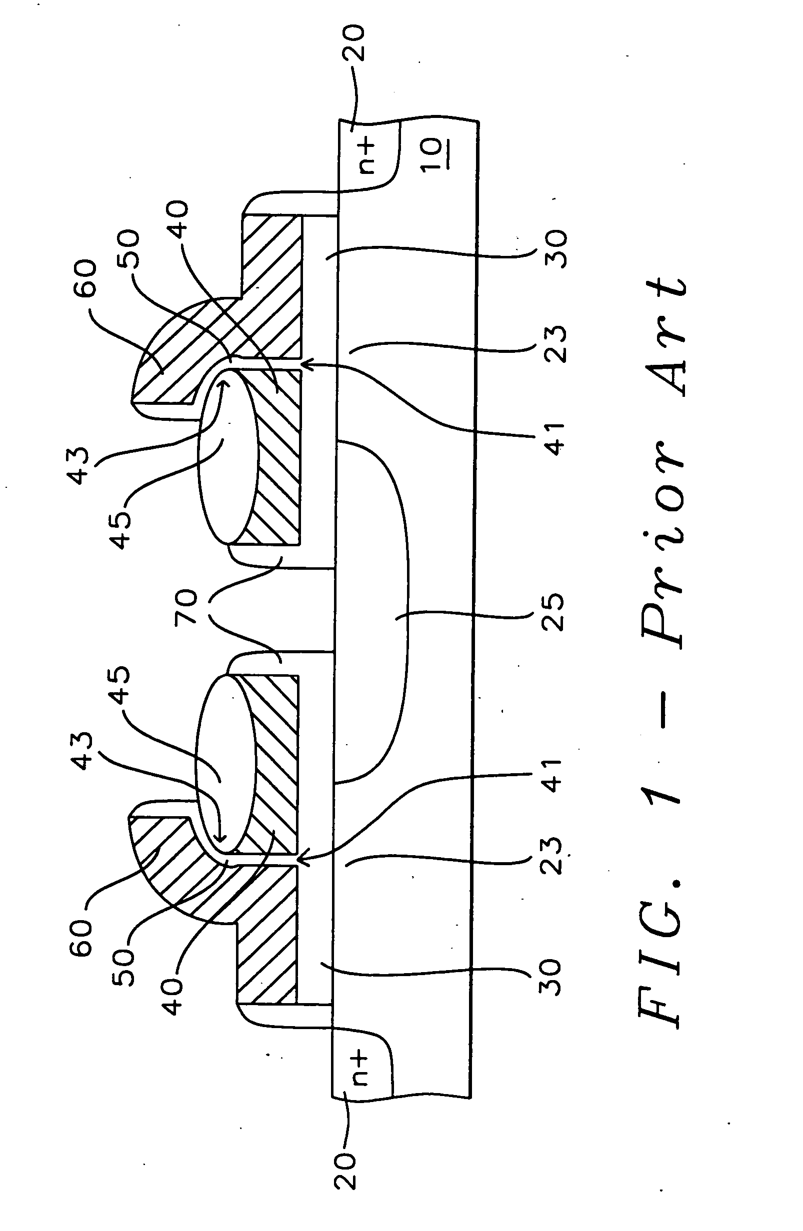
[0034] Referring now to the drawings, specifically to FIGS. FIGS. 4A-4H, and FIGS. 5A-5H, there is shown a preferred method of forming a split-gate flash memory having a three-dimensional source capable of three-dimensional coupling with the floating gate of the cell. FIGS. 2A-2H and FIGS. 3A-3H show the present state of manufacturing a split-gate flash memory cell. It will be apparent that the split-gate of FIGS. FIGS. 2A-2H and FIGS. 3A-3H lack the three-dimensional region of the trench of the preferred embodiment where three-dimensional coupling can take place between the floating gate and the source of this invention, as claimed later in the embodiments.

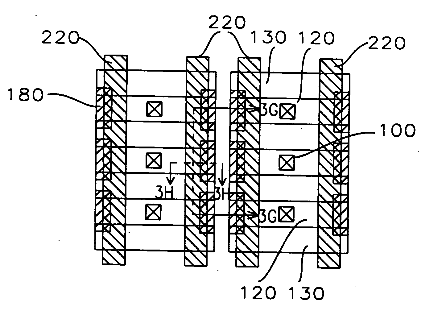
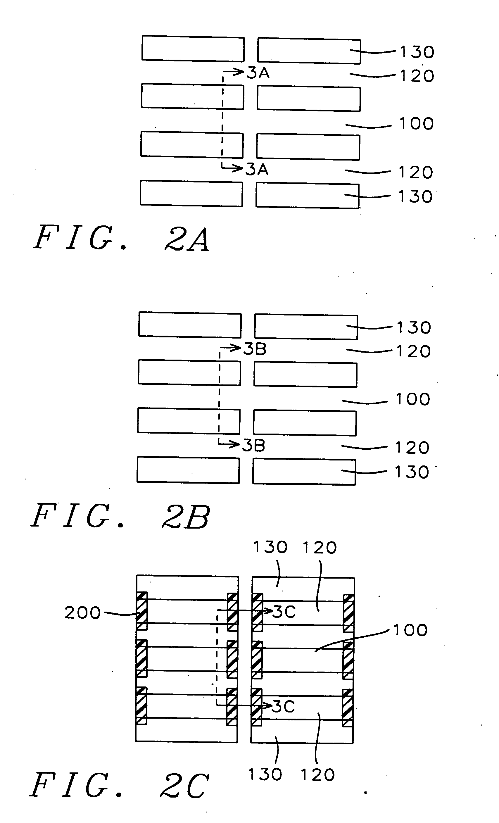
[0035]FIGS. 2A-2H show the top view of a semiconductor substrate on which various process steps are performed. Corresponding to each top view, a cross-sectional view of the substrate representing the results of a particular process step is shown in FIGS. 3A-3H.

[0036] Thus, FIG. 2A shows top view of a semiconductor substrate (10...


PUM


Abstract

A split-gate flash memory cell having a three-dimensional source capable of three-dimensional coupling with the floating gate of the cell, as well as a method of forming the same are provided. This is accomplished by first forming an isolation trench, lining it with a conformal oxide, then filling with an isolation oxide and then etching the latter to form a three-dimensional coupling region in the upper portion of the trench. A floating gate is next formed by first filling the three-dimensional region of the trench with polysilicon and etching it. The control gate is formed over the floating gate with an intervening inter-poly oxide. The floating gate forms legs extending into the three-dimensional coupling region of the trench thereby providing a three-dimensional coupling with the source which also assumes a three-dimensional region. The leg or the side-wall of the floating gate forming the third dimension provides the extra area through which coupling between the source and the floating gate is increased. In this manner, a higher coupling ratio is achieved without an increase in the cell size while at the same time alleviating the punchthrough and junction break-down of source region by sharing gate voltage along the side-wall.

Description

BACKGROUND OF THE INVENTION [0001] (1) Field of the Invention [0002] The present invention relates to the manufacturing of semiconductor memories, and in particular, directed to a split-gate flash memory having an increased coupling ratio of source to floating gate and to a method of forming of the same. [0003] (2) Description of the Related Art [0004] The degree of coupling between a source and floating gate in a split-gate flash memory is determined by the capacity of source implant lateral diffusion under the floating gate. It is desirable to increase the coupling ratio because that results in improved programming speed. However, trying to increase coupling ratio by increasing the source implant lateral diffusion causes the well-known problems of punch-through and junction breakdown. It is disclosed later in the embodiments of this invention a method of increasing the coupling ratio of a split-gate memory cell by extending into the trench isolation region of the cell a three-dime...

Claims


Application Information

Patent Timeline
Patent Type & Authority Applications(United States)
IPC IPC(8): H01L21/336H01L21/8247H01L27/115H01L29/423H01L29/788
CPCH01L27/115H01L27/11521H01L29/7885H01L29/66825H01L29/42324H10B69/00H10B41/30
Inventor HSIEH, CHIA-TALIN, YAI-FENKUO, DI-SONSUNG, HUNG-CHENGYEH, JACK
Owner TAIWAN SEMICON MFG CO LTD
Why Eureka
Try Eureka