Metal-halogen physical vapor deposition for semiconductor device defect reduction

a technology of metal halogen physical vapor and semiconductor devices, which is applied in the direction of semiconductor devices, electrical appliances, basic electric elements, etc., can solve the problems of large leakage current, and inability to meet the requirements of the devi

Active Publication Date: 2005-09-22
TEXAS INSTR INC
View PDF8 Cites 15 Cited by
  • Summary
  • Abstract
  • Description
  • Claims
  • Application Information

AI Technical Summary

Problems solved by technology

Along with shrinking transistor geometries, however, also come a number of challenges to optimize both transistor and integrated circuit (IC) layout design.
Unfortunately a number of problems have been encountered when manufacturing transistors with nickel silicide source / drain electrodes.
In some cases, unacceptable numbers of nonfunctional transistors are constructed.
In other instances, the source and drain regions punch through the source / drain junction into the semiconductor substrate, resulting in a large leakage current.
In still other cases, there is an unacceptably large diode leakage between the source and drain regions and the semiconductor substrate.
These problems contribute to the production of unacceptably low yields of transistors that operate within performance specifications.

Method used


Image

  • Metal-halogen physical vapor deposition for semiconductor device defect reduction
  • Metal-halogen physical vapor deposition for semiconductor device defect reduction
  • Metal-halogen physical vapor deposition for semiconductor device defect reduction

Examples


Embodiment Construction

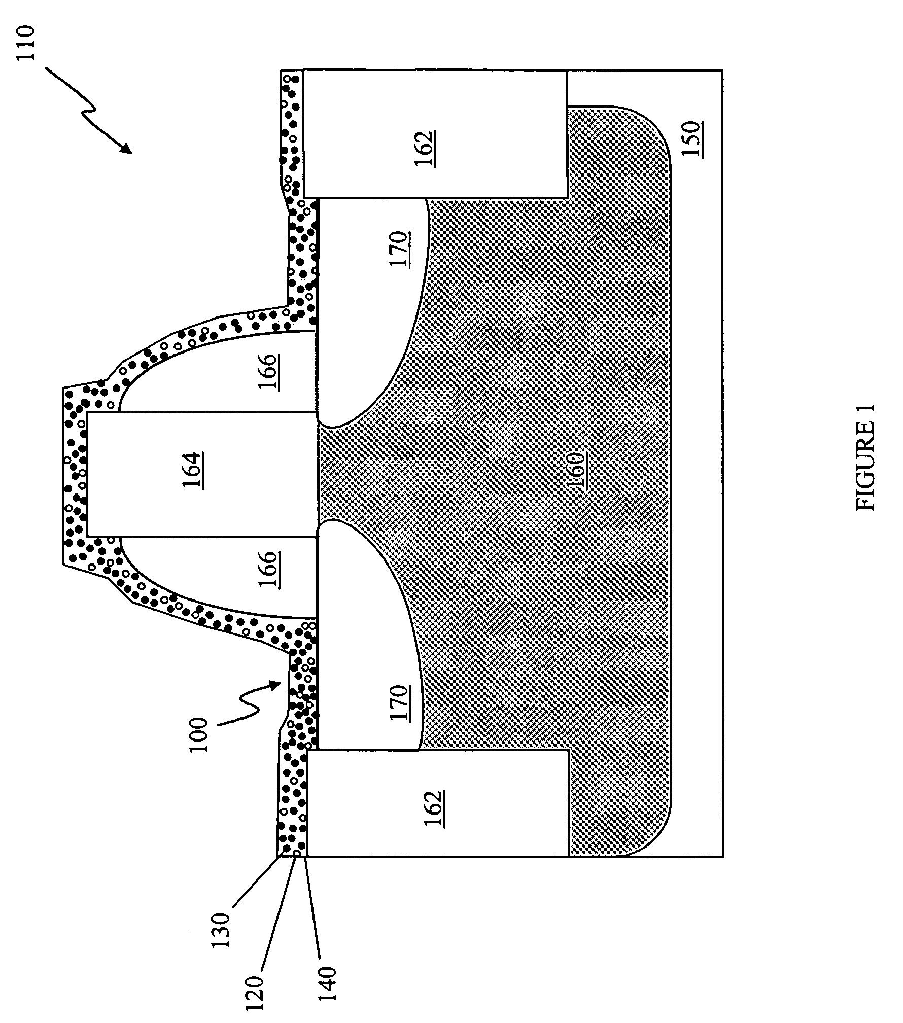
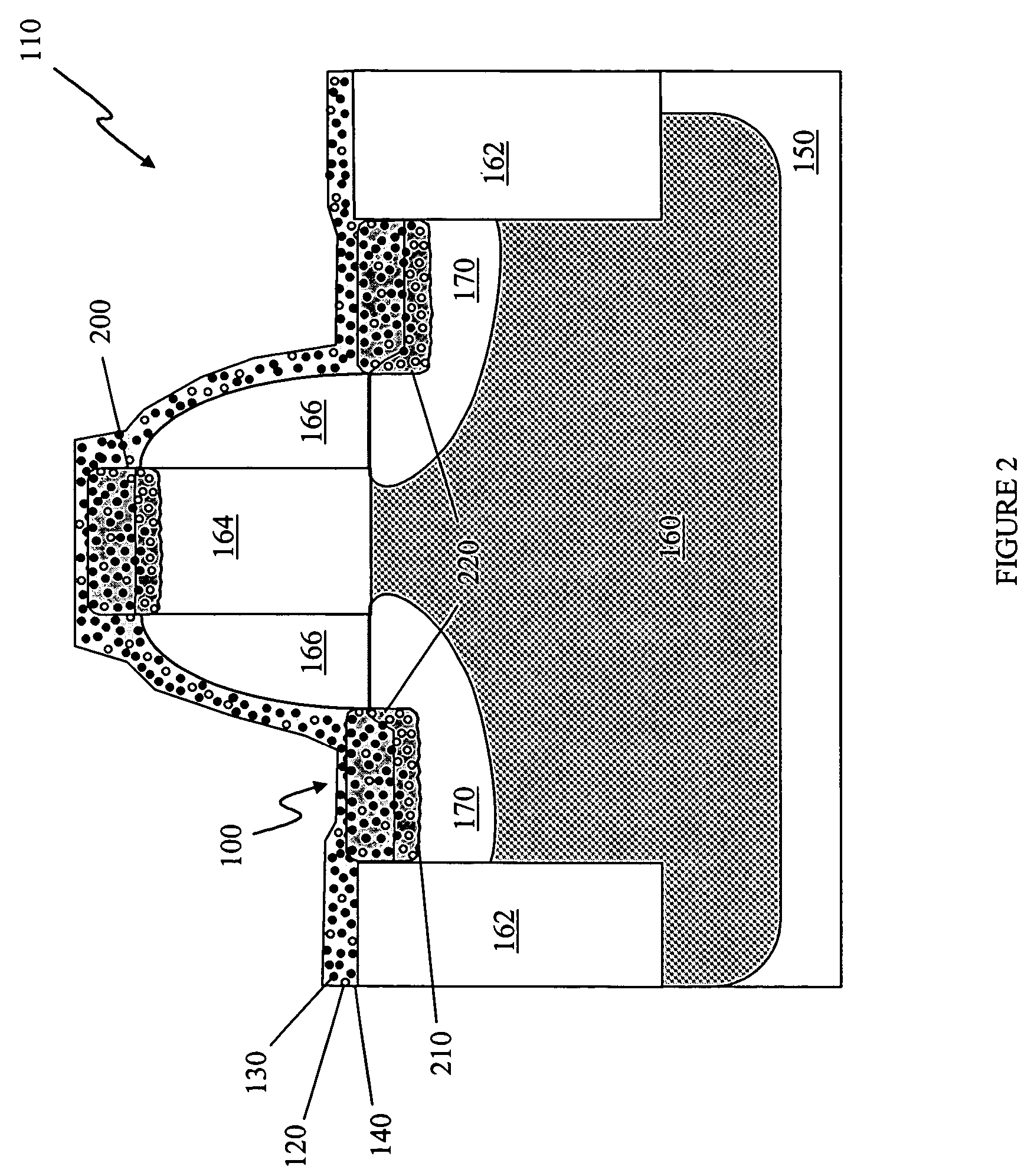
[0013] During the course of studying transmission electron microscope images (TEM) of MOS transistors having nickel silicide source / drain electrodes, spike-shaped and pipe-shaped defects due to excessive encroachment in both the vertical and lateral directions were detected. The vertical encroachment defects, mostly in the form of spikes, were portions of the source / drain electrodes that protruded into the silicon substrate below the source / drain region. The lateral encroachment defects, mostly in the form of pipes, were portions of the source / drain electrodes that protruded into the source / drain extension region of the transistor underneath the side wall spacer, and in some cases, beyond the source / drain into the channel region of the transistor. It is thought that the formation of these encroachment-related pipe and spike defects is due to the presence of favorable paths or channels in the source / drain regions and the silicon substrate that (locally) enhances the diffusion of nick...


PUM

PropertyMeasurementUnit
thicknessaaaaaaaaaa
thicknessaaaaaaaaaa
thicknessaaaaaaaaaa

Abstract

The present invention provides a method of manufacturing a metal silicide electrode (100) for a semiconductor device (110). The method comprises depositing by physical vapor deposition, halogen atoms (120) and transition metal atoms (130) to form a halogen-containing metal layer (140) on a semiconductor substrate (150). The halogen-containing metal layer and the semiconductor substrate are reacted to form a metal silicide electrode. Other aspects of the present invention include a method of manufacturing an integrated circuit (400) comprising the metal silicide electrode.

Description

CROSS-REFERENCE TO RELATED APPLICATIONS [0001] This application claims the benefit of U.S. Provisional Application U.S. Provisional Application No. 60 / 554,332 entitled, “INTEGRATED CIRCUIT METAL SILICIDE METHOD,” filed on Mar. 17, 2004 and which is commonly assigned with the present invention, and incorporated by reference as if reproduced herein in its entirety.TECHNICAL FIELD OF THE INVENTION [0002] The present invention is directed, in general, to a method for manufacturing a semiconductor device, and more specifically, to a method for manufacturing devices having metal silicide electrodes thereon. BACKGROUND OF THE INVENTION [0003] The continuing push to produce faster semiconductor devices with lower power consumption has resulted in transistor miniaturization and higher integrated circuit packing densities with each new technology node. For instance, transistors with smaller components allow a higher packing density, which is conducive to faster device operating speeds. Along ...

Claims


Application Information

Patent Timeline
Patent Type & Authority Applications(United States)
IPC IPC(8): H01L21/285H01L21/336H01L21/44H01L21/4763H01L21/8234H01L21/8238H01L29/78
CPCH01L21/28518H01L21/823418H01L21/823443H01L29/78H01L21/823835H01L29/665H01L21/823814
Inventor CHEN, PEIJUN J.YUE, DUOFENGMERCER, DOUGLAS E.RUSSELL, NOEL
Owner TEXAS INSTR INC
Why Eureka
Try Eureka