Nonvolatile memory

Inactive Publication Date: 2005-09-29
RENESAS TECH CORP
View PDF9 Cites 8 Cited by
  • Summary
  • Abstract
  • Description
  • Claims
  • Application Information

AI Technical Summary

Benefits of technology

[0011] Moreover, when a card reader may be used for a storage device comprising a plurality of data terminals, an amount of data to be transferred within the unit time may be increased in order to attain high speed data transfer by increasing data transfer rate or expanding bus width in data transfer. Here, it is desirable that the level of data terminal is determined with the determination circuit in such a timing that a command is inputted from an external circuit. Thereby, an increase of power consumption may be avoided by shortening the period during which the level of data terminal connected with

Problems solved by technology

As a result, it has become apparent that the number of terminals may be increased but here rises a problem that data read/write is impossible when

Method used


Image

  • Nonvolatile memory
  • Nonvolatile memory
  • Nonvolatile memory

Examples


first embodiment

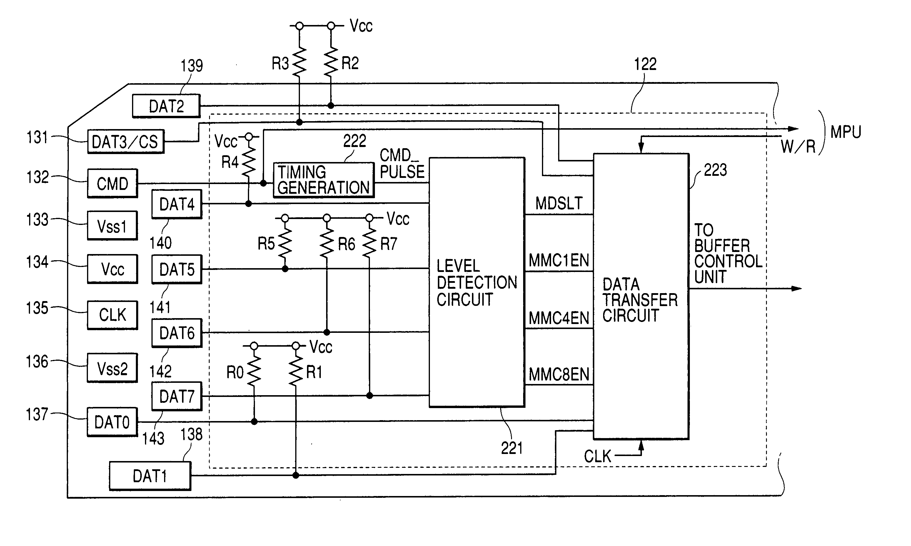
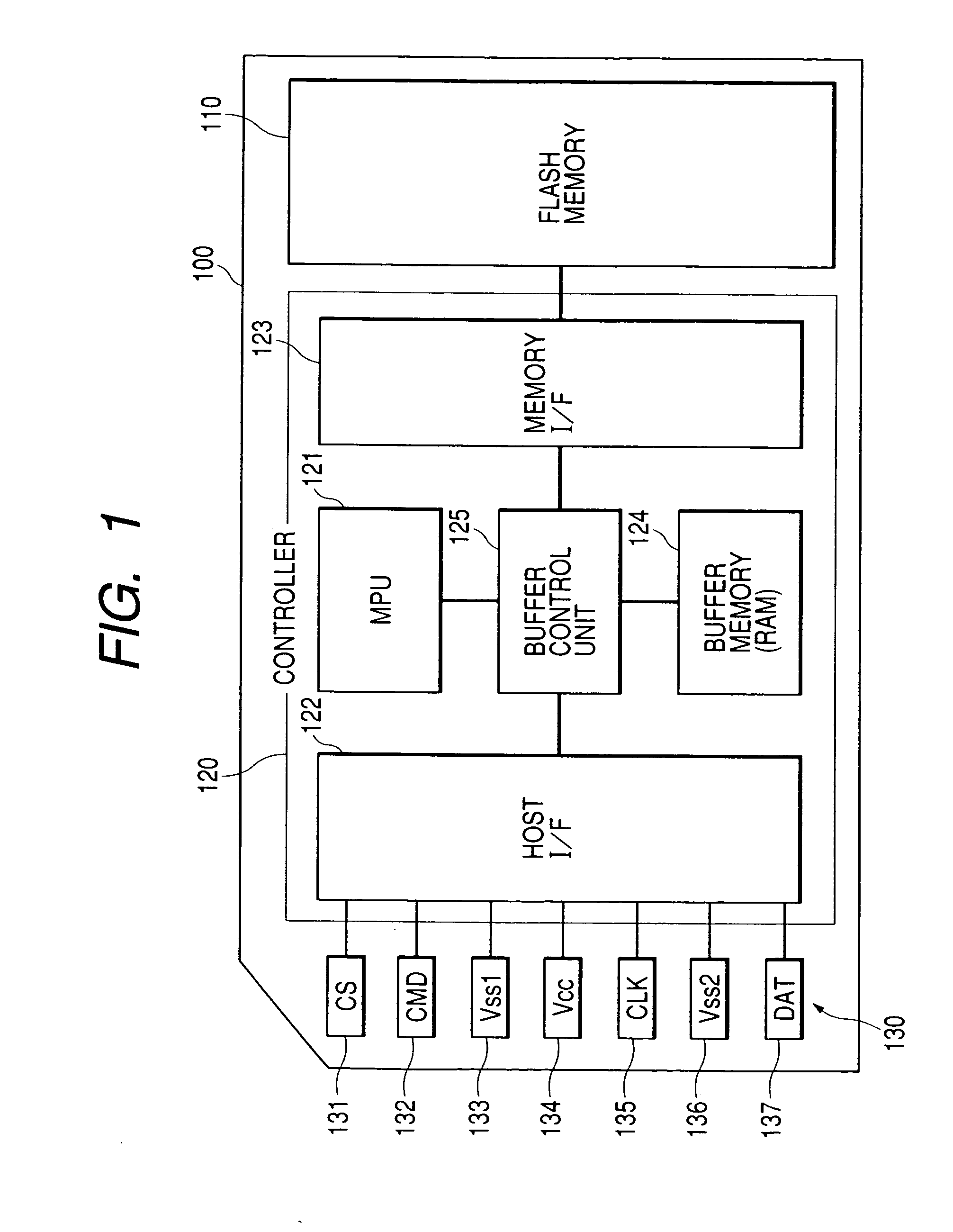
[0022]FIG. 1 illustrates a memory card comprising a nonvolatile memory to which the present invention is applied.

[0023] Although not particularly restricted, a memory card 100 in this embodiment is composed of a flash memory 110 which can simultaneously delete the data in the predetermined unit and a controller 120 for writing and reading data to and from the flash memory 110 based on the commands supplied from an external circuit. The flash memory 110 and controller 120 are respectively formed as semiconductor integrated circuits on different semiconductor chips. A memory card is formed by mounting these two semiconductor chips on a substrate not illustrated and then molding the entire part with a resin material or accommodating the entire part with a ceramic package or the like.

[0024] Moreover, the card is provided, on one side thereof, with an external terminal group 130 which is electrically connected to a circuit on the side of external device, when the card is inserted to a c...

second embodiment

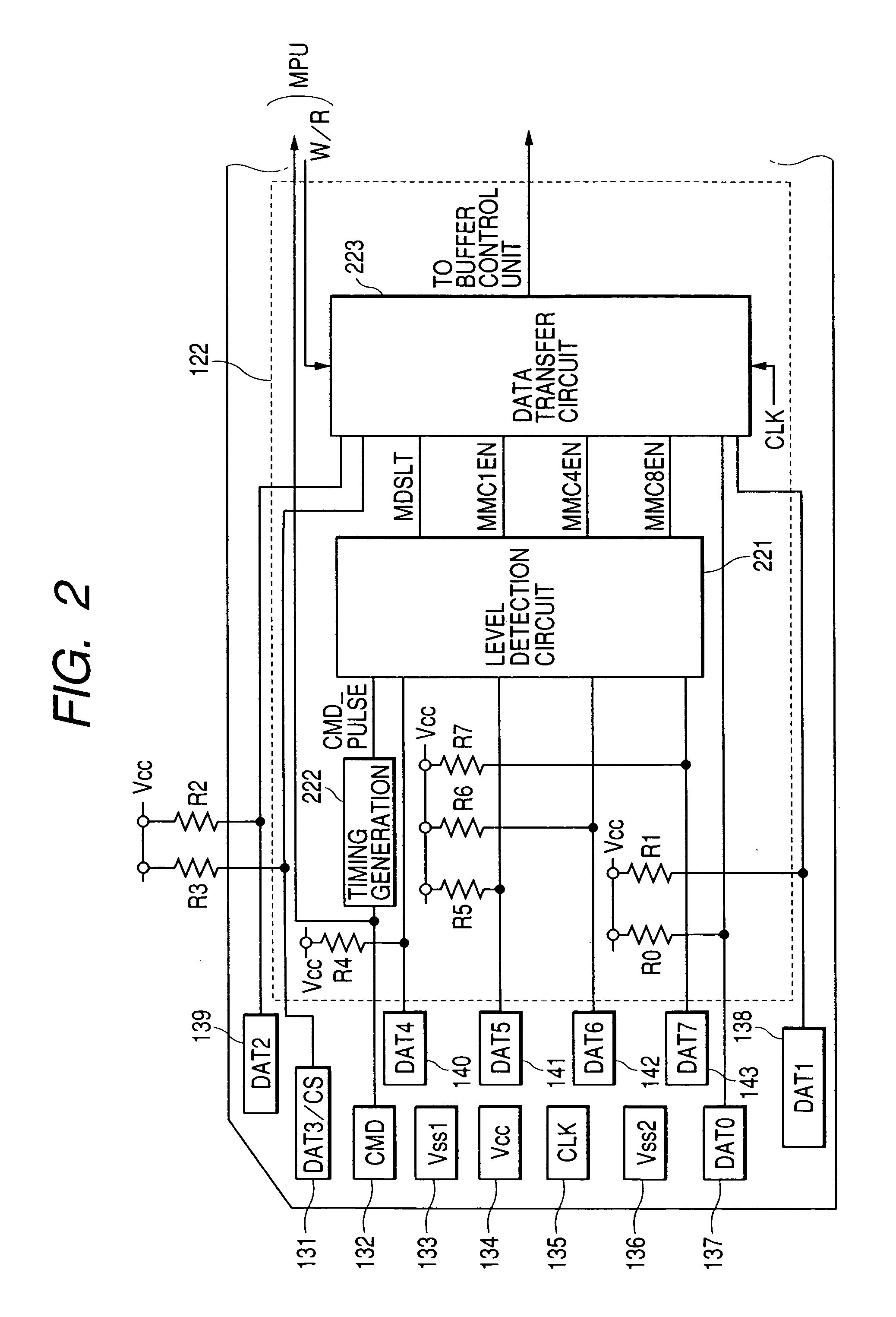
[0058] Next, the memory card of the present invention will be described with reference to FIG. 7 and FIG. 8.

[0059] The difference between the second embodiment and the first embodiment is that the level detection circuit 221 determines the operation mode from the conditions of the four external terminals 140 to 143 in the first embodiment, while the level detection circuit 221 determines the operation mode from the conditions of eight external terminals 131, 137 to 143 in the second embodiment. Therefore, in the second embodiment, the potential of the external terminals 131, 137 to 139 is also inputted to the level detection circuit 221, in addition to the potential of the external terminals 140 to 143. In addition, the level detection circuit 221 generates, depending on the conditions of these terminals, the eight signals DAT7EN to DAT0EN which indicate validity of input to the terminal and then supplies these signals to the data transfer circuit 223.

[0060] Accordingly, the memory...


PUM


Abstract

There is provided a technology to realize high speed data transfer while compatibility of a card type storage device comprising a nonvolatile memory is ensured. Namely, in the card type storage device comprising the nonvolatile memory, a plurality of data terminals are provided and an interface unit is provided with a circuit for determining levels of data terminals. Some or all of the plurality of data terminals are connected with pull-up resistors for pulling up to a power source voltage. When the determination circuit determines that the data terminals connected with the pull-up resistors are in an open condition, the determination circuit switches a bus width (number of bits) of data.

Description

BACKGROUND OF THE INVENTION [0001] The present invention relates to a technology which may be effectively applied to a nonvolatile storage device and more particularly to a technology which may be applied effectively to a card type storage device comprising a nonvolatile semiconductor memory, for example, a flash memory. [0002] In recent years, a card type storage device which is called a memory card comprising a nonvolatile memory such as a flash memory, which can store storage data even when supply of power source voltage is stopped, has been used widely as a data memory medium of a mobile electronic device such as a digital camera. [0003] In regard to the conventional memory card, data has generally been inputted and outputted serially between a card which is represented by a multimedia card (MultiMediaCard (registered trade mark) and a card reader. The reasons considered are that it is difficult, from the viewpoint of manufacture, to provide a sufficient number of external termi...

Claims


Application Information

Patent Timeline
IPC IPC(8): G06K19/06G06K19/07G06K19/077G11C5/02G11C7/00G11C16/04G11C16/06
CPCG06K19/07732G06K19/07A47F7/141A47F1/12
Inventor IIDA, TETSUYAKANAMORI, MOTOKISHIKATA, ATSUSHITAMURA, TAKAYUKIKATAYAMA, KUNIHIRO
Owner RENESAS TECH CORP
Why Eureka
Try Eureka