Semiconductor storage device and manufacturing method thereof

a technology of semiconductor storage device and semiconductor, applied in the direction of semiconductor device, electrical apparatus, transistor, etc., can solve the problems of insufficient thickness of thermal oxide film, insufficient reliability, and insufficient thickness to achieve the effect of thickness

Inactive Publication Date: 2005-09-29
SPANSION LLC
View PDF10 Cites 11 Cited by
  • Summary
  • Abstract
  • Description
  • Claims
  • Application Information

AI Technical Summary

Benefits of technology

[0010] As a result of assiduous studies, the inventors of the present application have found out that in a conventional manufacturing method of a semiconductor storage device, the formation of a large birds' beak, segregation of impurities, and the like occur because thermal oxidation is applied for forming an oxide film covering a stacked gate and so on. Then, the inventors of the present invention have found out that adopting plasma processing, instead of the thermal oxidation, as a method of forming a good-quality and precise insulating film can solve the disadvantages described above, and has come up with the following forms of the invention.

Problems solved by technology

Unstable characteristics of these insulating films may possibly produce a state in which some memory cell stores data of “1” while another memory cell stores data of “0”, even when the same control voltage is applied, resulting in extremely inferior reliability.
Therefore, this thermal oxide film is not uniform in thickness, and in order to fully prevent the entrance of the hydrogen even at the thinnest portion, the thickness to this extent is required.
However, in semiconductor storage devices formed by the above-described methods, birds' beaks are large to deteriorate coupling.
Such deterioration in coupling leads to a problem of deterioration in erase efficiency.
This deterioration in erase efficiency is especially noticeable in a memory where erase is conducted near an end portion of a gate electrode and in a memory where erase is conducted in the entire channel.
Moreover, if the birds' beak occurs, an insulating film becomes thick at that portion, which leads to deterioration not only in erase efficiency but also in data write efficiency.
There is another problem that it is difficult to stabilize characteristics of the finally manufactured semiconductor storage devices.
One of the causes thereof is that at the time of the thermal oxidation, a plurality of wafers are processed at a time, but it is very difficult to keep the temperature in a heating furnace constant at this time.
Another cause is that as a result of the thermal oxidation, impurities such as phosphorus which have been introduced into the floating gate and so on tend to segregate in peripheral edge portions thereof.

Method used


Image

  • Semiconductor storage device and manufacturing method thereof
  • Semiconductor storage device and manufacturing method thereof
  • Semiconductor storage device and manufacturing method thereof

Examples


first embodiment

[0030] (First Embodiment)

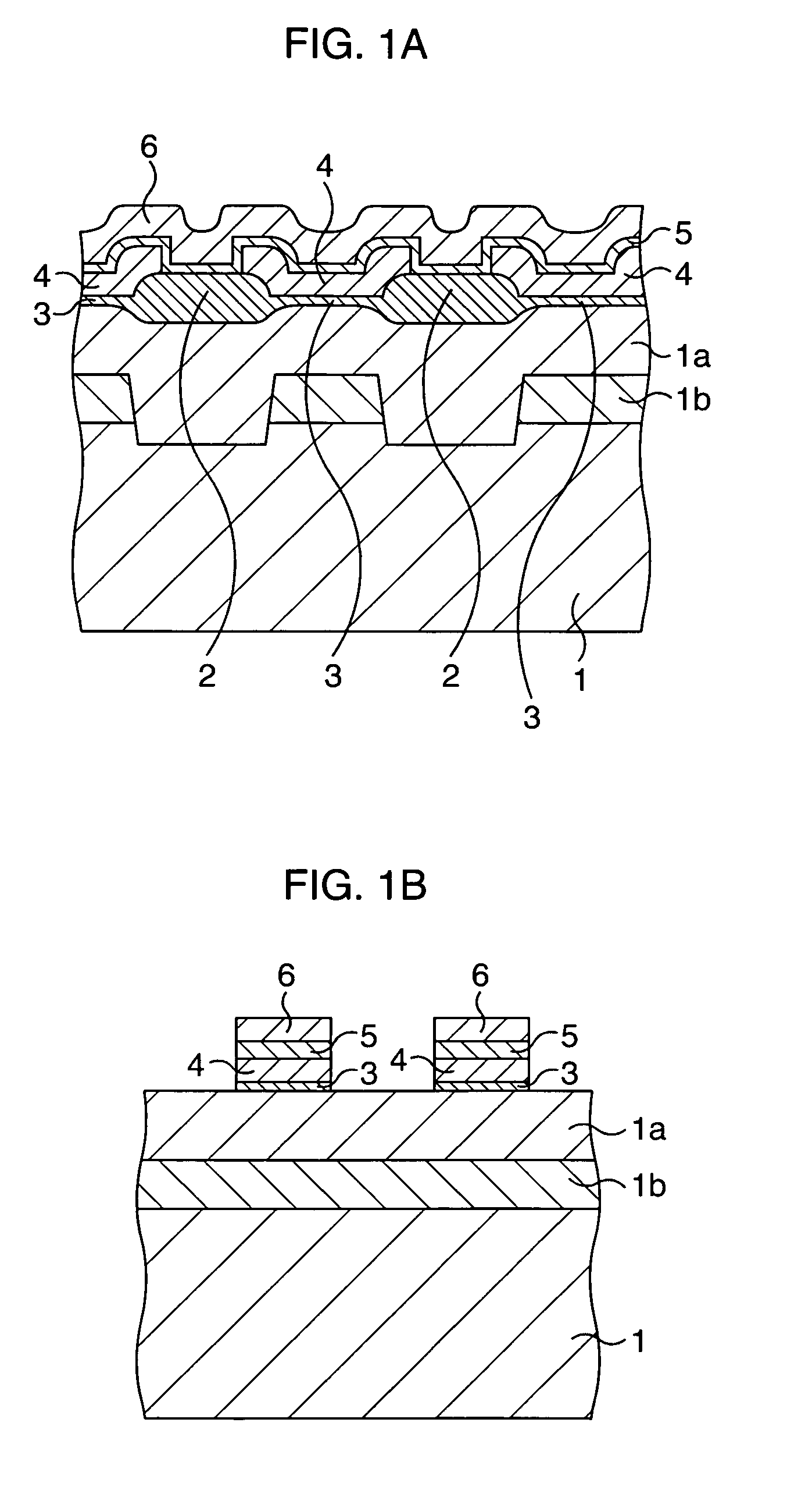
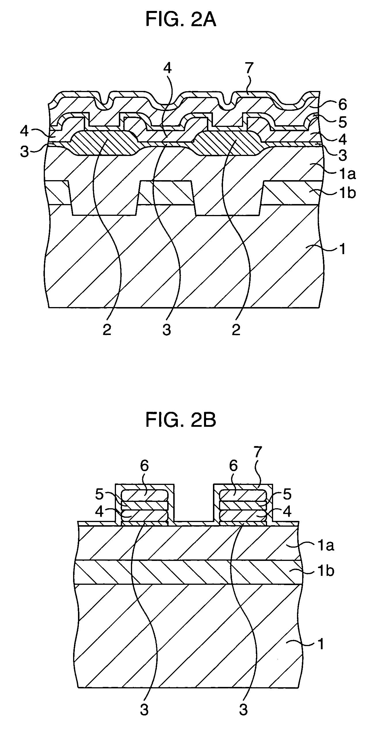
[0031] A first embodiment of the present invention will be first described. In the first embodiment, the present invention is applied to a semiconductor storage device with a stacked gate structure. FIG. 1A and FIG. 1B to FIG. 6A and FIG. 6B are cross-sectional views showing, in the order of steps, a manufacturing method of a semiconductor storage device according to the first embodiment of the present invention.

[0032] In the semiconductor storage device according to the first embodiment, a plurality of word lines and bit lines are formed in a grid so as to perpendicularly intersect each other. One memory cell is formed near each grid point. FIG. 1B to FIG. 6A correspond to a cross section perpendicular to the bit lines, and FIG. 1B to FIG. 6B correspond to a cross section perpendicular to the word lines. Therefore, FIG. 1A and FIG. 1B show cross sections perpendicular to each other. The same applies to the other FIG. 2A and FIG. 2B to FIG. 6A and FIG. 6B. ...

second embodiment

[0048] (Second Embodiment)

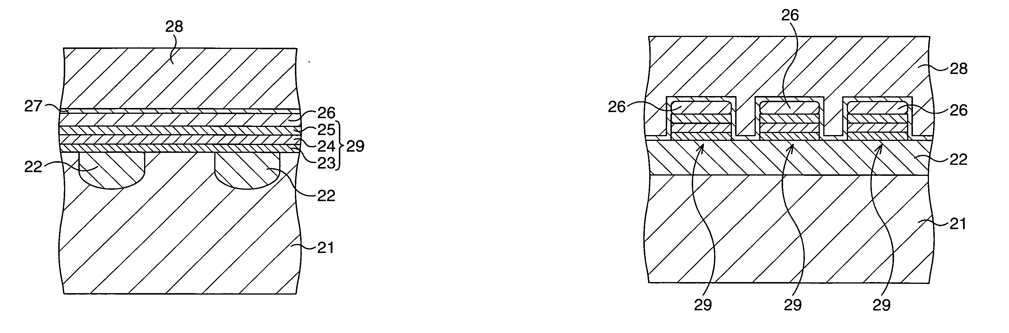
[0049] Next, a second embodiment of the present invention will be described. In the second embodiment, the present invention is applied to a semiconductor storage device with a so-called SONOS structure. FIG. 8A and FIG. 8B to FIG. 10A and FIG. 10B are cross-sectional views showing, in the order of steps, a manufacturing method of the semiconductor storage device according to the second embodiment of the present invention. The SONOS structure is a structure of a memory accumulating electric charges in a nitride film, which has sources / drains serving also as buried bit lines and channels parallel to word lines (gate electrodes), and it has a buried bit line structure.

[0050] Also in the second embodiment, a plurality of word lines and bit lines are formed in a grid so as to perpendicularly intersect each other. One memory cell is formed near each grid point. Similarly to the first embodiment, FIG. 8A to FIG. 10A correspond to a cross section perpendicular to...


PUM


Abstract

Tunnel insulating films (3) are formed in element regions demarcated by element isolation insulating films (2). Thereafter, for each memory cell, a floating gate (4) is formed, and an ONO film (5) and a control gate (6) are further formed. Next, a plasma insulating film (7) is formed on surfaces of stacked gates. The plasma insulating film is immune to plane orientation of a base film. Therefore, the entire plasma insulating film (7) has a substantially uniform thickness, and consequently, even if the maximum thickness thereof is not as large as that of a thermal oxide film, hydrogen entrance is prevented when the interlayer insulating film is thereafter formed, and electron leakage is also prevented. The reduction in thickness of this insulating film makes it possible to reduce birds' beaks, and efficiency in erase/write of data can be enhanced.

Description

TECHNICAL FIELD [0001] The present invention relates to a semiconductor storage device suitable as a flash memory and a manufacturing method thereof. BACKGROUND ART [0002] A flash memory is a nonvolatile semiconductor storage device that stores data by holding electric charges on a storage film such as a nitride film under a floating gate or a gate electrode. When the electric charges are accumulated on the floating gate, the electric charges are exchanged between a channel and the floating gate via a gate insulating film. When the electric charges are accumulated on the nitride film in an ONO film as the storage film, the electric charges are accumulated on an insulating film itself. Therefore, these insulating films are required to have stable electric characteristics. Unstable characteristics of these insulating films may possibly produce a state in which some memory cell stores data of “1” while another memory cell stores data of “0”, even when the same control voltage is applie...

Claims


Application Information

Patent Timeline
Patent Type & Authority Applications(United States)
IPC IPC(8): H01L21/28H01L21/8246H01L21/8247H01L27/115H01L29/51H01L29/788
CPCH01L21/28185H01L21/28194H01L21/28202H01L27/115H01L29/7883H01L27/11568H01L29/513H01L29/518H01L27/11521H10B43/30H10B69/00H10B41/30
Inventor UTSUNO, YUKIHIRONAKAMURA, MANABUSERA, KENTAROHIGASHI, MASAHIKONANSEI, HIROYUKITAKAGI, HIDEOKAJITA, TATSUYA
Owner SPANSION LLC
Why Eureka
Try Eureka