Distortion compensating device and power amplifying device with distortion compensating function

Inactive Publication Date: 2005-09-29
SNAPTRACK
View PDF1 Cites 39 Cited by
  • Summary
  • Abstract
  • Description
  • Claims
  • Application Information

AI Technical Summary

Benefits of technology

[0023] The distortion compensating device and the power amplifying device with a distortion compensating function in the present invention do not adjust the phase of the second harmonic for distortion compensation, which is injected to the power amplifier, by the phase shift circuit as in the conventional manner, but adjust the impedance of the

Problems solved by technology

Consequently, the output of as high a power as possible particularly in a state of a low power-supply voltage leads to low power consumption in the entire terminal.
However, when the switching power threshold is made higher, distortion is increased, so that reducing the distortion in the low output is an important issue.
Although distortion compensation te

Method used


Image

  • Distortion compensating device and power amplifying device with distortion compensating function
  • Distortion compensating device and power amplifying device with distortion compensating function
  • Distortion compensating device and power amplifying device with distortion compensating function

Examples


first embodiment

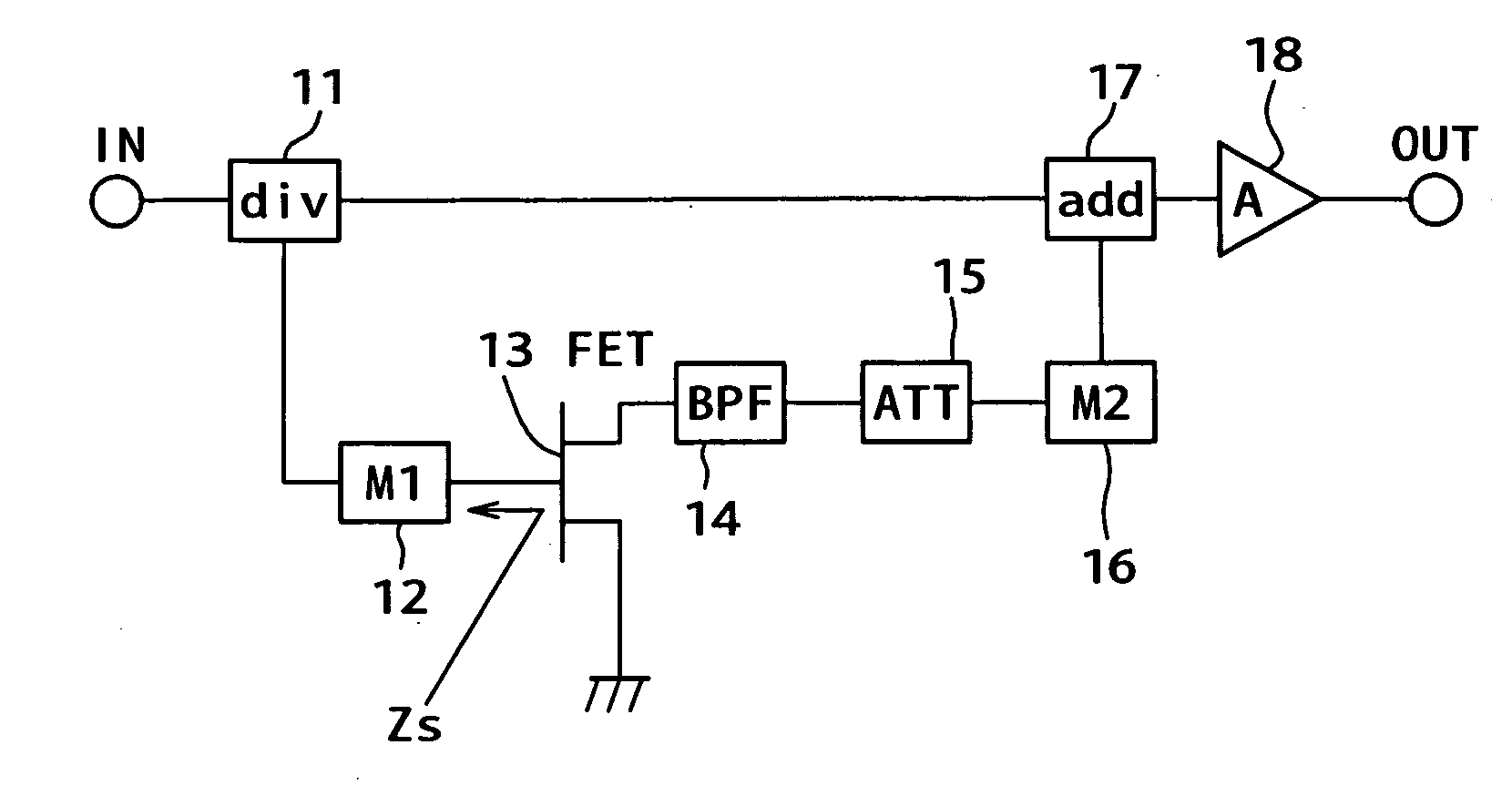
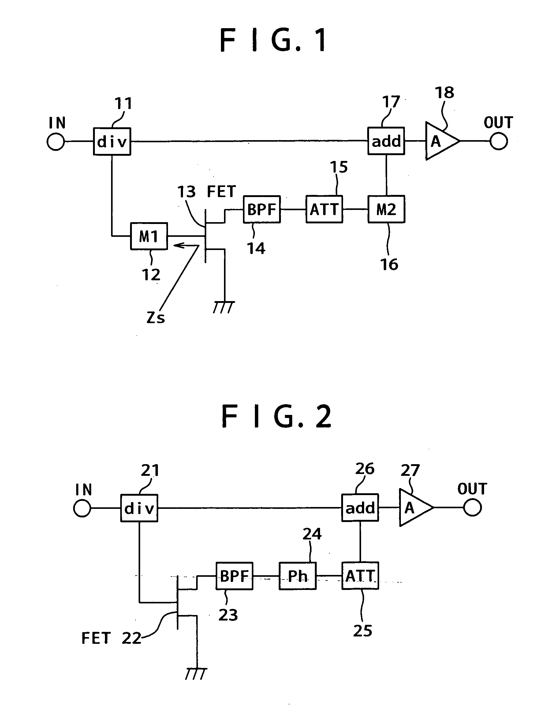
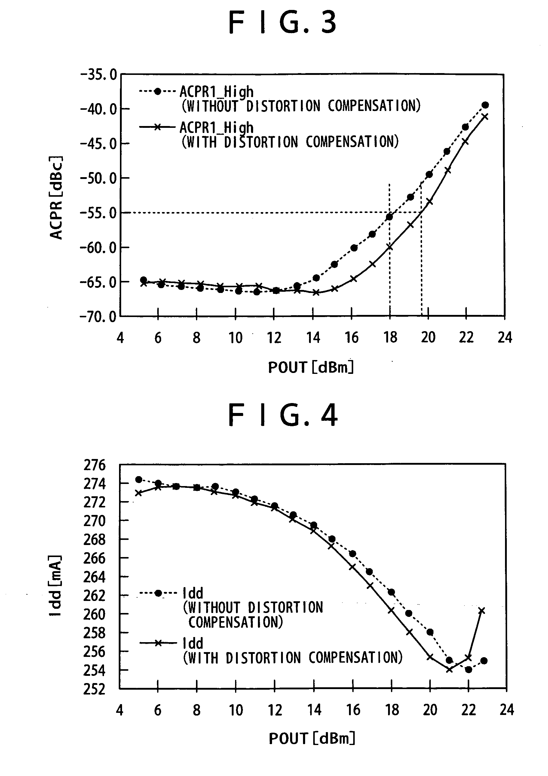
[0033]FIG. 1 is a circuit block diagram of the present invention. A configuration is first described. This circuit composes a distortion compensating device for compensating distortion generated by a power amplifier (A) 18. The distortion compensating device includes: a dividing circuit (div) 11 which divides an input signal inputted in an input terminal IN into two; a source grounded FET 13; a first matching circuit (M1) 12 connected between a first output terminal of the dividing circuit 11 and a gate terminal of the FET 13; a band pass filter (BPF) 14 which is connected to a drain terminal of the FET 13 to pass only a second harmonic; an attenuation circuit (ATT) 15 which is connected to the output of this band pass filter 14 to attenuate a signal voltage of the second harmonic; a second matching circuit (M2) 16 connected to output of the attenuation circuit 15; and an addition circuit (add) 17 in which the output of the second matching circuit 16 is connected to a first input te...

second embodiment

[0042]FIG. 7 is a circuit block diagram showing a configuration example of a power amplifying device according to the present invention. For reference, a configuration of a conventional typical power amplifier having no distortion compensating function is shown in FIG. 8. The power amplifier shown in FIG. 8 is a two-stage power amplifying circuit including two source grounded FETS, in which a first matching circuit 51, a first source grounded FET 52, a second matching circuit 53, a second source grounded FET 54 and a third matching circuit 55 are series-connected from an input terminal In to an output terminal OUT.

[0043] In contrast to the configuration of FIG. 8, the configuration of the second embodiment is first described, referring to FIG. 7. This power amplifying device includes an input terminal IN, a first matching circuit 31, a first source grounded FET 32, a dividing circuit 33, a band pass filter (BPF) 35, an attenuation circuit (ATT) 36, a second matching circuit 37, a th...


PUM


Abstract

One divided signal divided into two by a dividing circuit is inputted to a gate of a source grounded FET through a first matching circuit. In a drain of the FET, a second harmonic having a phase and an amplitude in accordance with an impedance of the first matching circuit is generated and extracted in a band pass filter and then the amplitude is adjusted in an attenuation circuit to input to an addition circuit through a second matching circuit. In the addition circuit, the output of the second matching circuit is added to another divided signal of the dividing circuit and inputted to a power amplifier. The impedance in the first matching circuit affecting the phase of the second harmonic generated from the FET is set so that a distortion component generated in the power amplifier is compensated for by the second harmonic inputted in the addition circuit.

Description

CROSS REFERENCE TO RELATED APPLICATIONS [0001] The present document is based on Japanese Priority Document JP2004-032351, filed in the Japanese Patent Office on Feb. 9, 2004, the entire contents of which being incorporated herein by reference. BACKGROUND OF THE INVENTION [0002] 1. Field of the Invention [0003] The present invention relates to a distortion compensating device and more particularly to a distortion compensating device applicable to a high frequency power amplifier and a power amplifying device with a distortion compensating function. [0004] 2. Description of the Related Art [0005] Generally speaking, in a mobile telephone employing a CDMA (Code Division Multiple Access) system, the transmission power of a terminal is constantly fluctuating and the peak of output distribution is in the vicinity of about 10 mW in the case where voice is used. Therefore, in many of the CDMA mobile telephone terminals, the power-supply voltage of a power amplifier (PA) is changed between l...

Claims


Application Information

Patent Timeline
IPC IPC(8): H03F1/32H03F3/24H04B1/04
CPCH03F1/3276
Inventor KUSUNOKI, SHIGEOKAWAKAMI, KATSUJI
Owner SNAPTRACK
Why Eureka
Try Eureka