Method and composite hard mask for forming deep trenches in a semiconductor substrate

a technology of semiconductor substrate and composite hard mask, which is applied in the direction of semiconductor devices, electrical apparatus, transistors, etc., can solve the problems of increasing fabrication costs, degrading fabrication yields, and difficult removal of undoped silicate glass layers, so as to achieve easy and complete removal

Active Publication Date: 2005-09-29
NAN YA TECH
View PDF2 Cites 5 Cited by
  • Summary
  • Abstract
  • Description
  • Claims
  • Application Information

AI Technical Summary

Benefits of technology

[0022] According to the present invention, the borophosphosilicate glass layer and the borosilicate glass layer formed on the borophosphosilicate glass layer serve as a hard mask for forming deep trenches in the semiconductor substrate. While most boron in the borophosphosilicate glass layer will diffuse upward in a direction toward the borosilicate glass layer after the semiconductor structure being subject to an annealing process, little phosphorus diffuse upward. Abundant phosphorus doped in the borophosphosilicate glass layer enables the borophosphosilicate glass layer to be easily and completely removed away from the semiconductor substrate by using the vapor of hydrogen fluoride.

Problems solved by technology

In comparison with a doped silicate glass layer, the un-doped silicate glass layer is more difficult to be removed by using the vapor of hydrogen fluoride.
The results shown in both FIGS. 3A and 3B adversely influence the subsequent processes, increase the fabrication costs and may degrade the fabrication yields.
Attempt has been made to avoid the conditions shown in FIGS. 3A and 3B by omitting the annealing process in the aforementioned trench forming process, however, this would result in defective profiles of the deep trenches.
However, the approach of omitting the annealing process to prevent the boron in the borosilicate glass layer 18 from diffusing upward, in order to obtain better hard mask removal, would result in abnormal critical dimensions of the deep trenches for the 0.11-micron technology generation, for example, inconsistent width of deep trenches 28′ and 28″ as depicted in FIG. 4.

Method used


Image

  • Method and composite hard mask for forming deep trenches in a semiconductor substrate
  • Method and composite hard mask for forming deep trenches in a semiconductor substrate
  • Method and composite hard mask for forming deep trenches in a semiconductor substrate

Examples


Embodiment Construction

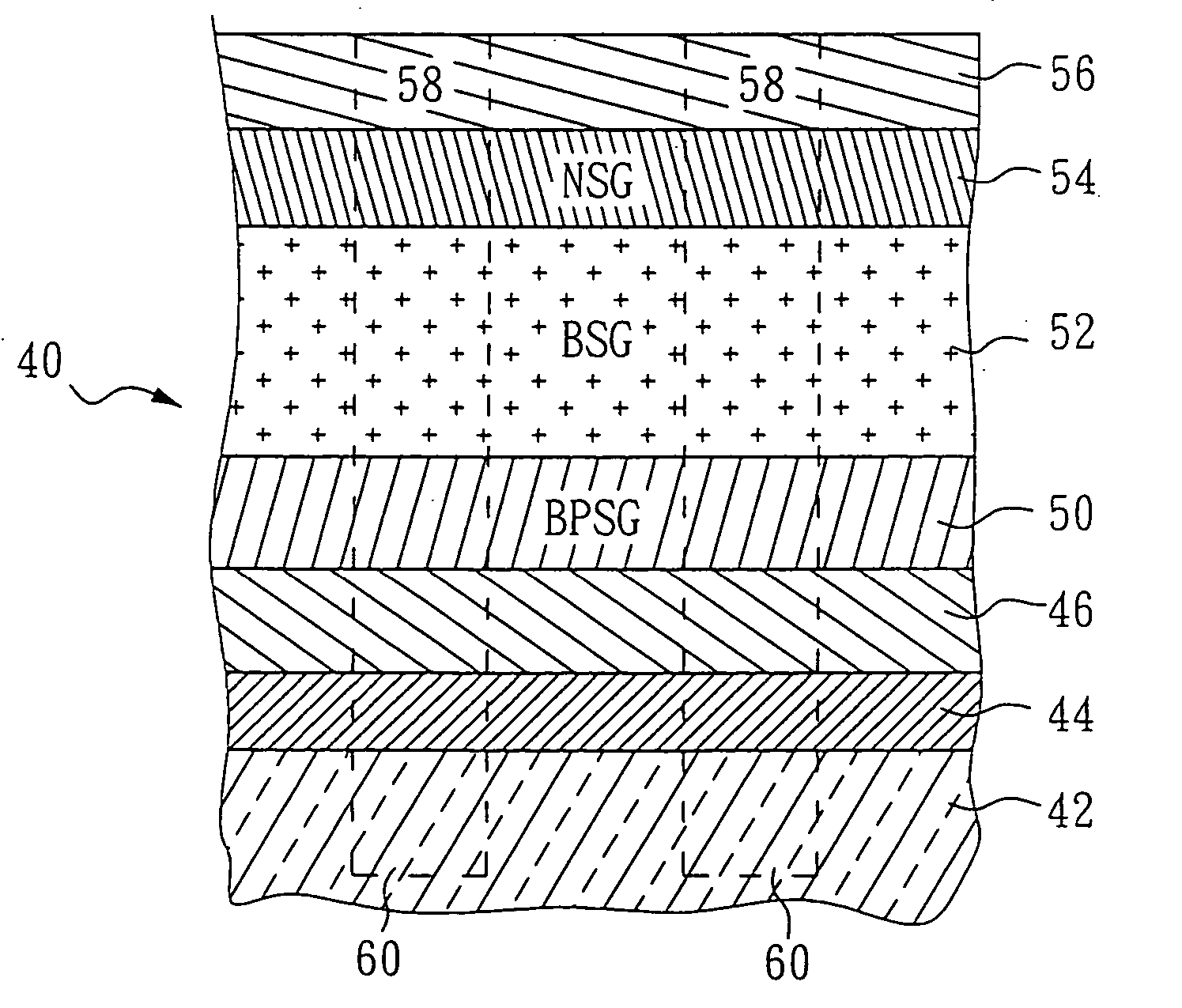
[0033]FIG. 5 shows a cross-sectional view of an electronic structure 40 having deep trenches made by a method according to the present invention. The electronic structure 40 comprises: a pad oxide layer 44 on a semiconductor substrate 42; a pad nitride layer 46 on the pad oxide 44; a borophosphosilicate glass layer 50 on the pad nitride layer 46; and a borosilicate glass layer 52 on the borophosphosilicate glass layer 50.

[0034] The semiconductor substrate 42 includes semiconductor material, such as silicon. The pad oxide layer 14 and pad nitride layer 16 both can be formed by any conventional means. The borophosphosilicate glass layer 50 and borosilicate glass layer 52, both of which function as a composite hard mask can be formed by any conventional means, such as thin film deposition technology. An un-doped silicate layer 54 may also be deposited on the borosilicate glass layer 52 to serve as a protection layer. Followed the formation of hard mask, the electronic structure 40 is ...


PUM

PropertyMeasurementUnit
anisotropicaaaaaaaaaa
anti-humidityaaaaaaaaaa
temperatureaaaaaaaaaa

Abstract

A method and structure for forming deep trenches in a semiconductor substrate is provided. The method comprises: providing a semiconductor substrate; forming a pad oxide layer on the semiconductor substrate; forming a pad nitride layer on the pad oxide layer; forming a borophosphosilicate glass layer on the pad nitride layer; forming a borosilicate glass layer on the borophosphosilicate glass layer; and forming deep trenches through the borosilicate glass layer, through the borophosphosilicate glass layer, through the pad nitride, through the pad oxide, and into the semiconductor substrate. The borosilicate glass layer and the borophosphosilicate glass layer function as a composite hard mask in forming the deep trenches. With the borophosphosilicate glass layer, the composite hard mask can be easily removed by dry etch process using hydrogen fluoride vapor after the deep trenches have been formed.

Description

FIELD OF THE INVENTION [0001] The present invention relates to a method and composite hard mask for forming deep trenches in a semiconductor substrate, particularly to the utilization of a novel composite hard mask in deep trench etching process. BACKGROUND OF THE INVENTION [0002] In fabricating semiconductor devices, trenches are formed in a semiconductor substrate to isolate active devices therein, or serve in part as a structure for fabricating dynamic random access memory (DRAM). The process for fabricating the trench typically includes defining an opening of the trench through a photolithography process and performing an anisotropic etching. Subsequent processes may be carried out according to the material characteristics of the semiconductor device. [0003] FIGS. 1 to 4 are cross-sectional views of a conventional semiconductor structure 10 illustrating deep trenches formed in a semiconductor substrate 12 by a known method. As shown in FIG. 1, a conventional method of forming th...

Claims


Application Information

Patent Timeline
Patent Type & Authority Applications(United States)
IPC IPC(8): H01L21/033H01L21/20H01L21/308H01L21/31H01L21/311H01L21/334H01L21/469H01L21/762H01L21/8242
CPCH01L21/0332H01L29/66181H01L21/76224H01L21/3081
Inventor WU, CHANG-RONGCHEN, YINANTSAI, TUZ-CHING
Owner NAN YA TECH
Why Eureka
Try Eureka