

Semiconductor wafers with non-standard crystal orientations and methods of manufacturing the same
a technology of silicon wafers and crystal orientations, which is applied in the direction of crystal growth process, polycrystalline material growth, chemically reactive gases, etc., can solve the problems of restricting the properties of devices made with monocrystalline silicon wafers, and the crystal structure of wafers to certain orientations
- Summary
- Abstract
- Description
- Claims
- Application Information
AI Technical Summary
Problems solved by technology
Method used
Image

Examples
first embodiment
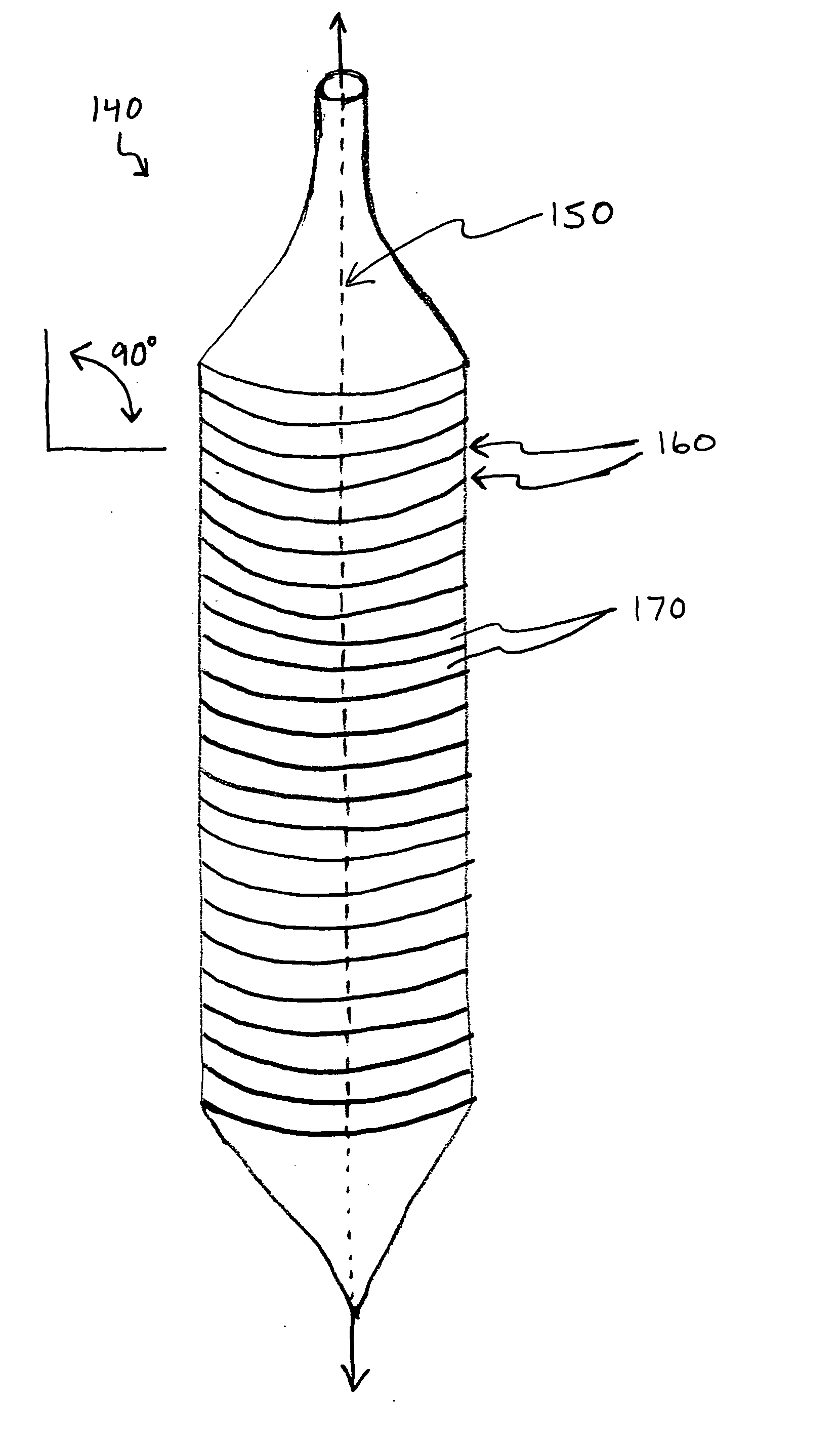
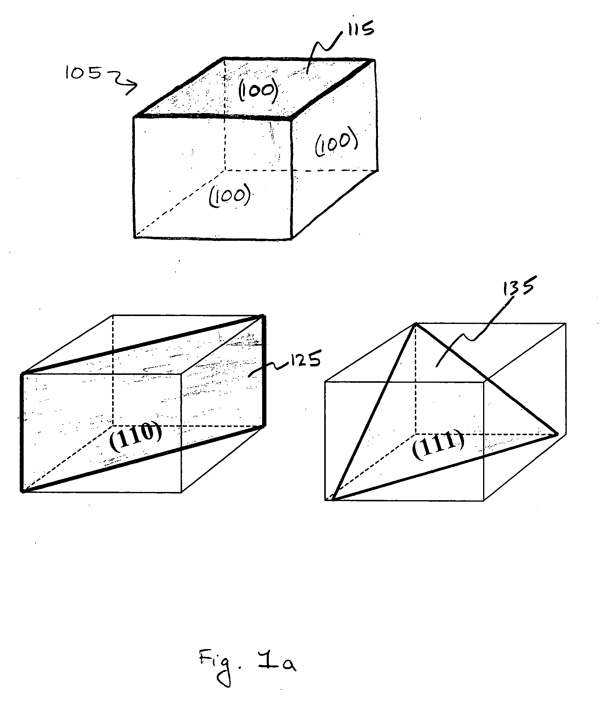
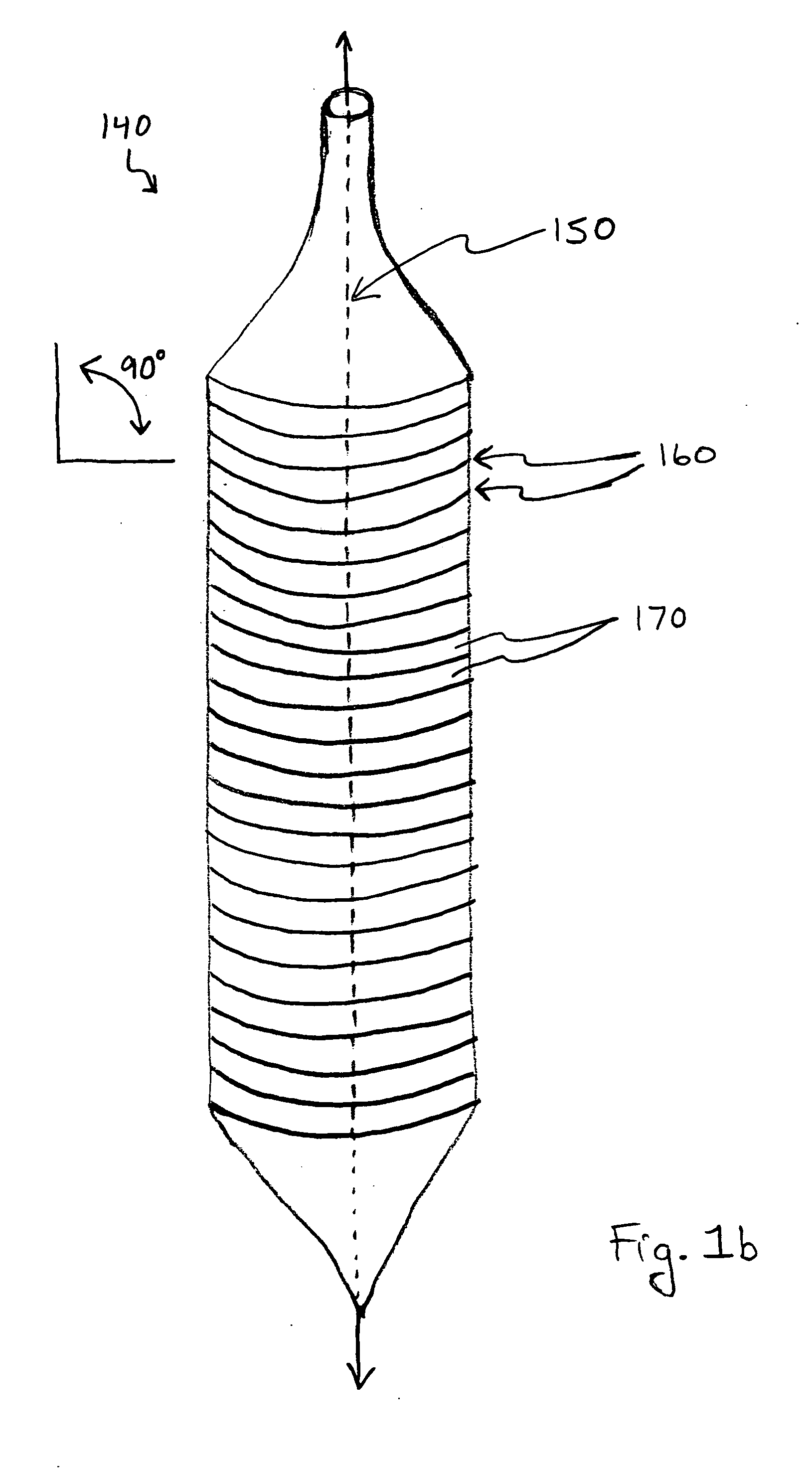
[0024] After the monocrystalline semiconductor ingot 300 has been formed to have a particular crystal orientation, in forming a semiconductor substrate having a non-standard crystal orientation at 220, the ingot 300 is sliced crosswise at approximately a 90 degree angle from the lengthwise axis 310 of the ingot 300, as illustrated in FIG. 3a, to form the wafer 320. Many wafers 320 may be sliced from the ingot 300, each having a thickness in the approximate range from 375 microns to 800 microns, depending on the diameter of the wafer. For a wafer having a diameter of approximately 300 mm the thickness of the wafer may be in the approximate range of 750 microns to 800 microns. At 230, after slicing the wafer 320 from the ingot 300, the wafer 320 is marked at a position to form an orientation indication feature, such as a notch or a flat, that is at an angle of greater than 0 degrees from a crystal plane perpendicular to the horizontal surface of the wafer. FIG. 4a illustrates a partic...
second embodiment
[0025] At 240, in forming a semiconductor substrate having a non-standard crystal orientation, the ingot 300 may be sliced at an angle other than 90 degrees from the lengthwise axis 310 of the ingot. As illustrated in FIG. 3b, the ingot 300 may be sliced at an angle by angling the cutting device 330 relative to the ingot 300 while the ingot 300 is mounted in a standard position. Alternatively, this ingot may be cut at an angle other than 90 degrees from the lengthwise axis 310 of the ingot 300 by keeping the cutting device 330 that is used to cut the ingot 300 in the standard position and angling the mounting position of the ingot 300 prior to slicing, as illustrated in FIG. 3c. As illustrated in FIG. 3b, for example, the ingot may be sliced at an angle of 45 degrees from the lengthwise axis 310. In a particular embodiment, the ingot may be sliced at an angle in the approximate range of 0.01 degrees and 10 degrees to maintain the roundness of the wafer.
[0026] At 250, after slicing t...
third embodiment
[0027] At 260, in forming a semiconductor substrate having a non-standard crystal orientation at 260, the ingot 300 may be sliced at an angle other than 90 degrees from the lengthwise axis 310 of the ingot, as described above. Then, at 270, the wafer 320 may be marked at a position to form an orientation indication feature that is at an angle of greater than 0 degrees from a crystal plane perpendicular to the horizontal surface of the wafer, also as described above.
PUM
| Property | Measurement | Unit |
|---|---|---|
| angle | aaaaa | aaaaa |
| angle | aaaaa | aaaaa |
| angle | aaaaa | aaaaa |
Abstract
Description
Claims
Application Information