Display device

a display device and display tube technology, applied in the direction of identification means, discharge tubes, luminescnet screens, etc., can solve the problems of display devices that continue to suffer from problems and difficulties, and achieve the effect of reducing the length of the driver lin

Inactive Publication Date: 2005-10-06
138 EAST LCD ADVANCEMENTS LTD
View PDF15 Cites 58 Cited by
  • Summary
  • Abstract
  • Description
  • Claims
  • Application Information

AI Technical Summary

Benefits of technology

[0032] It can be appreciated that for large area displays, difficulties arise whether active or passive driving schemes are adopted and these difficulties become more problematical when organic or polymer LEDs are used as the display light emitting elements. For very large area displays, such as for example those used to display images in public places, it is known to combine a number of displays to provide the very large area display. However, each display making up part of such a very large area display is a separate display device. Whilst the use of a large number of display devices can reduce the length of the driver lines in comparison to an equivalent size display made up of a single display device, each display device of the large area display nevertheless includes the relatively long address lines for addressing the light emitting elements of the display. As such these display devices continue to suffer from the concerns outlined above. Therefore, there is a significant need to provide an improved type of display device in which the above concerns are alleviated.

Problems solved by technology

It can be appreciated that for large area displays, difficulties arise whether active or passive driving schemes are adopted and these difficulties become more problematical when organic or polymer LEDs are used as the display light emitting elements.
As such these display devices continue to suffer from the concerns outlined above.

Method used


Image

  • Display device
  • Display device
  • Display device

Examples


Embodiment Construction

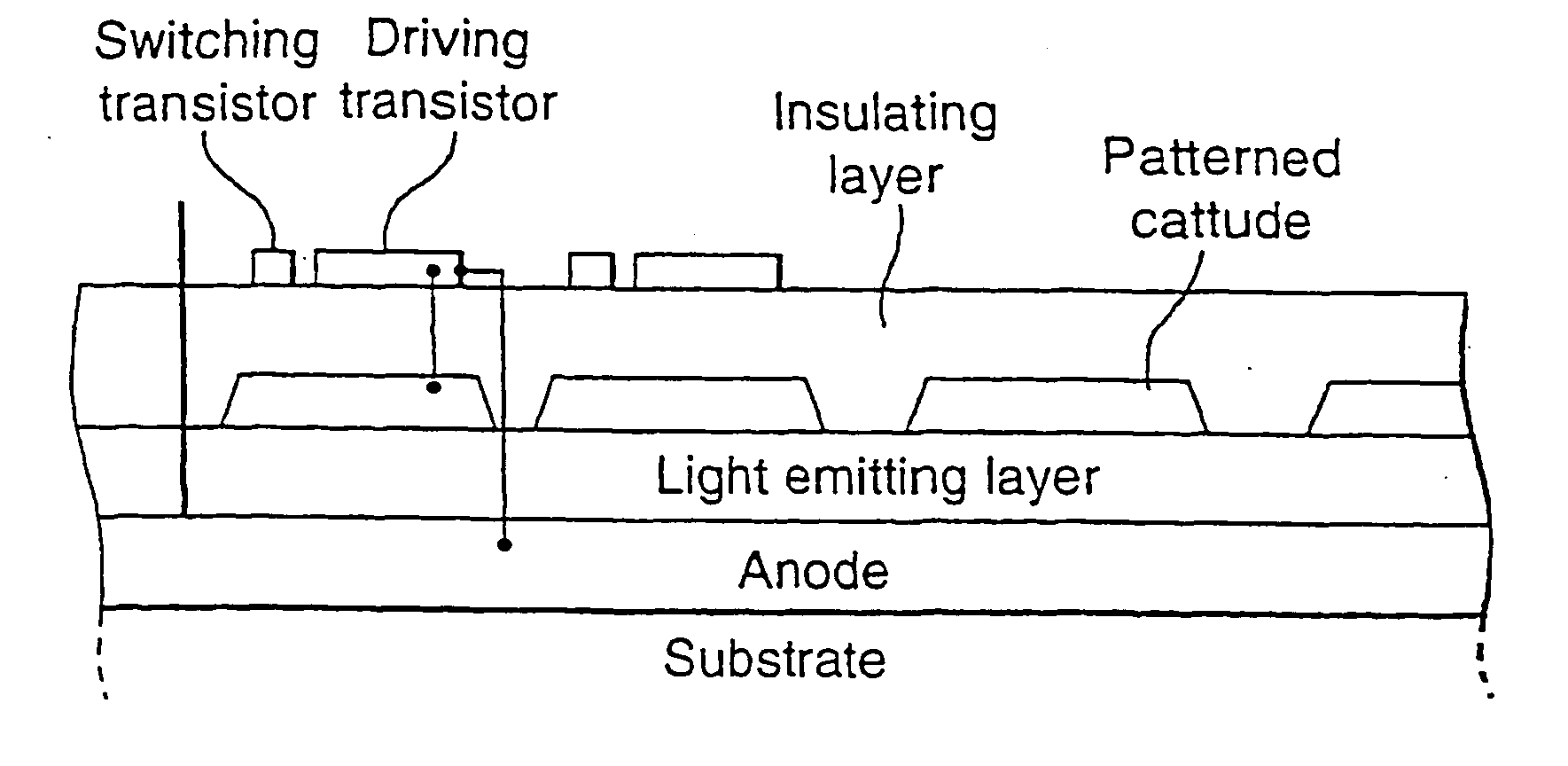
[0069] For a liquid crystal display, the liquid crystal material, being a fluid material, must be contained between a substrate and a front plate or panel for the display. Hence, the addressing lines and the driver transistors (if an active matrix is used) are located between the substrate and front plate within the liquid crystal material itself, as shown in FIG. 6. With such a construction, the liquid crystal pixels must, in practice, be driven from the edges of the display, otherwise, it becomes necessary to gain access to the addressing lines by providing holes through the front and rear panels of the display, which is not a practical proposition.

[0070] It follows that, with a liquid crystal display, as the size of the display area is increased, the length of the addressing lines will also increase, and the displays will suffer from the addressing problems described above, irrespective of whether an active or a passive matrix addressing scheme is adopted.

[0071] In an organic o...


PUM


Abstract

The invention provides a display device (26) including a plurality of discrete display segments (2). Each display segment (2) is provided with a drive circuit for driving the display elements arranged within the display area. The display device may be provided either as a passive, active or direct pixel addressed array. By interconnecting a number of display segments, a large area display can be achieved without the requirement for long electrodes. This reduces the electrical resistance and parasitic capacitance of the addressing electrodes, enabling the display to provide improved luminance in a displayed image and to operate at higher speeds, providing improved resolution. An active matrix addressing scheme can also be implemented using relatively low mobility organic thin film transistors.

Description

CROSS-REFERENCE TO RELATED APPLICATION [0001] This is a Division of application Ser. No. 10 / 276,597 filed Nov. 19, 2002, which is a National Stage of Application No. PCT / GB02 / 00412, filed Jan. 30, 2002. The entire disclosure of the prior applications is hereby incorporated by reference herein in their entirety.BACKGROUND OF THE INVENTION [0002] 1. Field of Invention [0003] The present invention relates to display devices and, in particular, to driver arrangements for display devices. [0004] 2. Description of Related Art [0005] A variety of display devices, such as liquid crystal displays or light emitting diode (LED) displays, are in widespread use. Recently, a further type of LED display has been proposed in the form of an addressable electroluminescent display. The electroluminescent display device comprises a mix of organic materials such as organic polymers or small molecules sandwiched between an anode and a cathode supported by a solid substrate, such as, for example, a glass,...

Claims


Application Information

Patent Timeline
Patent Type & Authority Applications(United States)
IPC IPC(8): G09F9/30H01L51/50H01L21/336H01L27/08H01L27/28H01L27/32H01L29/786H01L51/05H05B33/26
CPCH01L27/3262H01L27/3274G02F1/13336H01L27/3293H01L51/0508H01L27/3281H10K59/129H10K59/125H10K59/17H10K59/18H10K59/1213H10K10/46H05B33/00
Inventor KAWASE, TAKEO
Owner 138 EAST LCD ADVANCEMENTS LTD
Why Eureka
Try Eureka