Liquid crystal display device and method for fabricating the same

a technology of liquid crystal display and liquid crystal, which is applied in the direction of static indicating devices, ornamental textile articles, instruments, etc., can solve the problems of light leakage, low power consumption of lcd devices, and general light weight of lcd devices, so as to reduce the number of processing steps and simplify the manufacturing process

Active Publication Date: 2005-10-06
LG DISPLAY CO LTD
View PDF7 Cites 27 Cited by
  • Summary
  • Abstract
  • Description
  • Claims
  • Application Information

AI Technical Summary

Benefits of technology

[0027] Another advantage of the present invention is to provide an LCD device in which the manufacturing process is simplified.
[0028] An advantage of the present invention is to provide a liquid crystal device and a method for manufacturing the same, in which the number of processing steps are reduced by patterning a overcoat layer, a passivation layer, and a gate insulation layer in the same processing step.
[0029] To achieve these and other advantages and in accordance with the purpose of the present invention, as embodied and described herein, an LCD device comprises a gate line and a gate pad on a substrate; a gate insulating layer on an entire surface of the substrate including the gate line except the gate pad; a data line and a data pad on the gate insulating layer; a thin film transistor at a crossing portion of the gate line and the data line; a passivation layer on the entire surface of the substrate including the thin film transistor except the gate pad and data pad; an overcoat layer on the passivation layer, the overcoat layer; a pixel electrode in contact with the thin film transistor through a contact hole formed in the passivation layer and the overcoat layer; a first transparent conductive layer for contacting and covering the gate pad; and a second transparent conductive layer for contacting and covering the data pad.
[0030] To achieve these and other advantages and in accordance with the purpose of the present invention, as embodied and de

Problems solved by technology

Also, LCD devices are generally light in weight and consume low power compared to CRTs (Cathode Ray Tubes), and LCD devices can be used in notebook computer

Method used


Image

  • Liquid crystal display device and method for fabricating the same
  • Liquid crystal display device and method for fabricating the same
  • Liquid crystal display device and method for fabricating the same

Examples


first embodiment

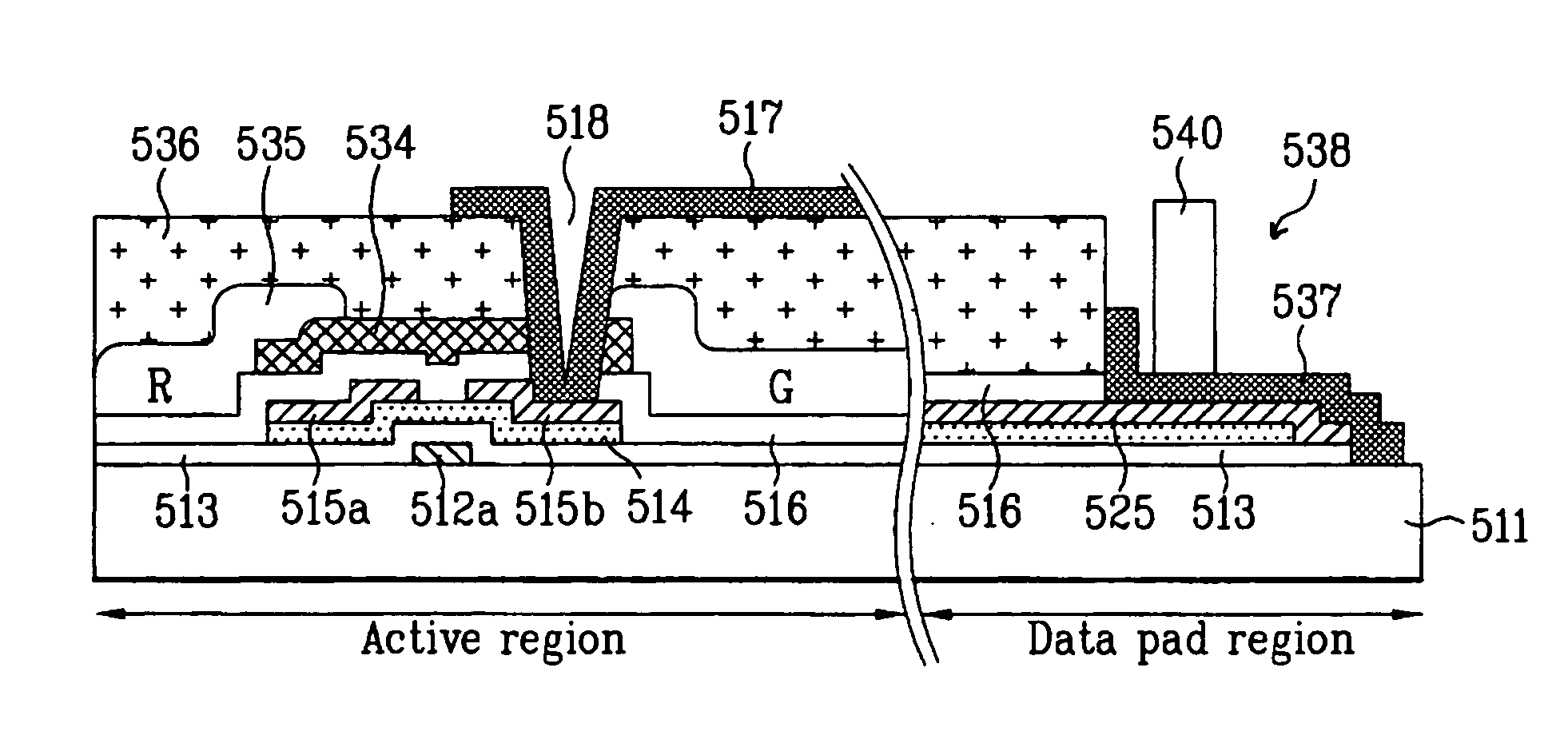
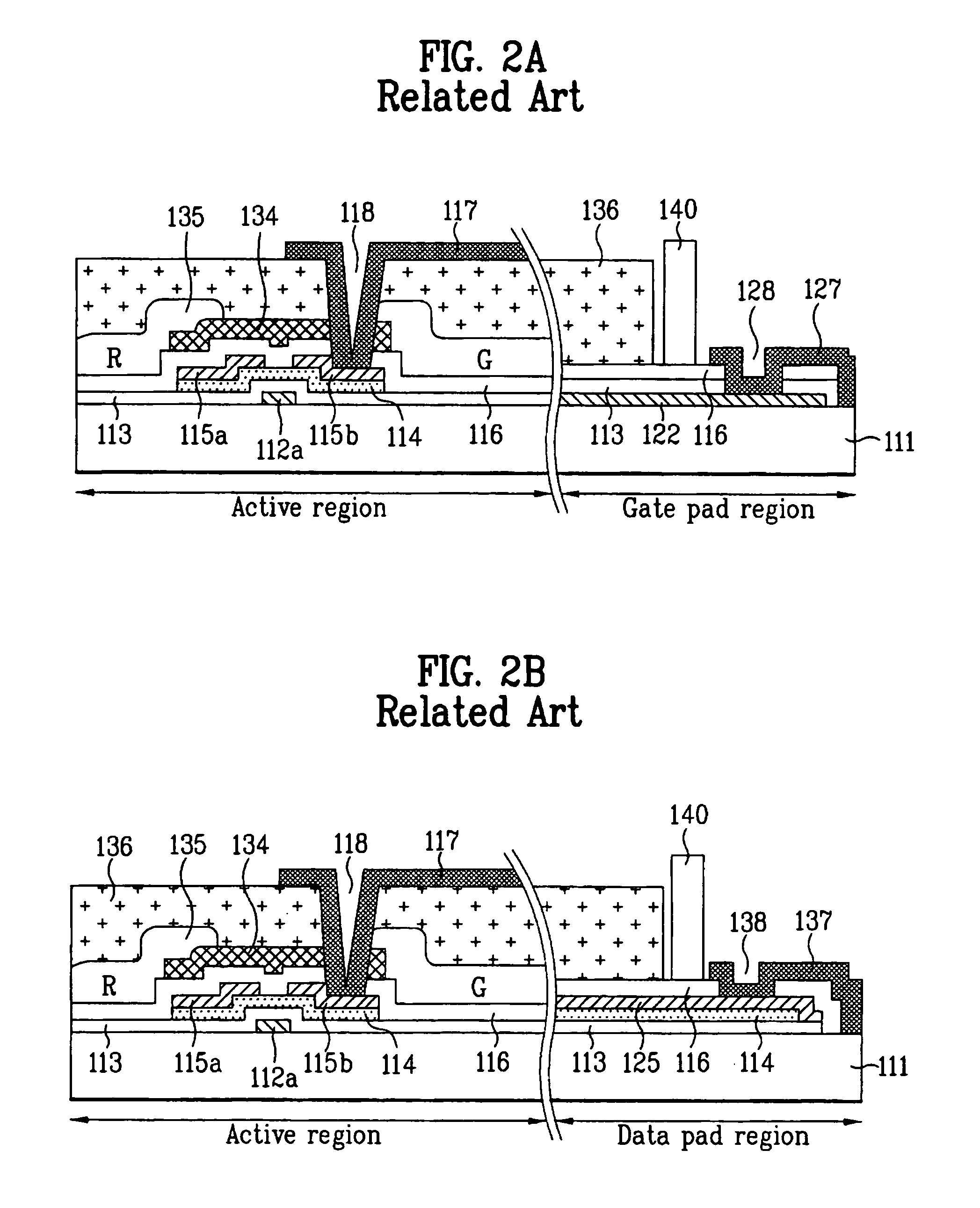
[0046]FIG. 5A and FIG. 5B are cross sectional views illustrating a COT type LCD device according to the present invention. As illustrated in FIG. 5A and FIG. 5B, a color filter layer and a thin film transistor TFT are formed on one substrate 511. The substrate 511 includes an active region, a gate pad region, and a data pad region. The color filter layer 535 and the TFT are formed in the active region of the substrate 511. Also, a gate pad 522 is formed in the gate pad region, and a data pad 525 is formed in the data pad region.

[0047] Referring to FIG. 5A and 5B, on the active region of the substrate 511 are a gate line (not shown), a gate insulating layer 513, a semiconductor layer 514, a data line (not shown), source / drain electrodes 515a / 515b, and a passivation layer 516. The gate line (not shown) having a gate electrode 512a is formed along one direction on the substrate 511, and the gate insulating layer 513 is formed on an entire surface of the substrate 511 including the gate...

second embodiment

[0063] The LCD device according to the present invention includes a substrate 511, the gate metal 532, a gate insulating layer 513, a data pad 525, a passivation layer 516, an overcoat layer 536, and a second transparent conductive layer 537. The gate metal 532 is additionally formed on the data pad region of the substrate 511. Also, the gate insulating layer 513 is formed on the substrate 511 and overlapping a portion of the gate metal 532. The data pad 525 extending from a data line (not shown) is formed on the gate insulating layer 513. The passivation layer 516 and the overcoat layer 536 are disposed on the data pad 525. The second transparent conductive layer 537 prevents the gate metal 532 from being exposed and being oxidized. In addition, the second transparent conductive layer 537 electrically connects the gate metal 532 with the data pad 525.

[0064] Herein, the gate metal 532 is formed substantially in an island shape and at the same layer as a gate line of the active regio...

third embodiment

[0071] The LCD device according to the present invention includes a gate line (not shown), a gate electrode 1512a, a gate pad 1522, a gate insulating layer 1513, a data line (not shown), a data pad 1525, the thin film transistor TFT, a passivation layer 1516, a overcoat layer 1536, a pixel electrode 1517, a first transparent conductive layer 1527, and a second transparent conductive layer 1537. The gate insulating layer 1513 is formed on an entire surface of the substrate 1511 including the gate line (not shown), and the data line (not shown) and the data pad 1525 are formed on the gate insulating layer 1513. Also, the TFT is formed at a crossing portion of the gate line and the data line, and the passivation layer 1516 is formed on the entire surface of the substrate 1511 including transistor TFT. Then, the overcoat layer 1536 is formed on the entire surface of the substrate 1511 including the passivation layer 1516, wherein the overcoat layer 1536 has substantially the same patter...


PUM


Abstract

An LCD device and a method for manufacturing the same is disclosed in which the manufacturing process is simplified by etching an overcoat layer and a lower insulating layer at the same time. Disclosed is a method for manufacturing the LCD device that includes forming a thin film transistor (TFT) on an active region of a substrate, forming a gate pad region and data pad region, and forming a passivation layer on the entire surface of the substrate. The manufacturing method further includes forming an overcoat layer and selectively etching the overcoat layer. Contact holes for the pixel electrode, the gate pad, and the data pad are formed by selectively etching the overcoat layer, the passivation layer, and the gate insulating layer though one process.

Description

[0001] This application claims the benefit of the Korean Application No. P2004-22625 filed on Apr. 1, 2004, which is hereby incorporated by reference for all purposes as if fully set forth herein. BACKGROUND OF THE INVENTION [0002] 1. Field of the Invention [0003] The present invention relates to a liquid crystal display (LCD) device, and more particularly, to an LCD device in which a color filter array and a TFT array are formed on one substrate. [0004] 2. Discussion of the Related Art [0005] Recently, LCD devices have gained in popularity as flat display devices, due to advantageous characteristics such as high contrast ratio, excellent gray level, high picture quality, and low power consumption. For example, LCD devices may be used in ultra-thin display device applications, such as wall-mountable televisions. Also, LCD devices are generally light in weight and consume low power compared to CRTs (Cathode Ray Tubes), and LCD devices can be used in notebook computers operated by bat...

Claims


Application Information

Patent Timeline
IPC IPC(8): G02F1/133G02F1/136G02F1/1362H01L21/77H01L21/84H01L27/12H01L29/786
CPCG02F1/13458H01L27/1288H01L27/124G02F1/136227D04D9/00D04D7/06D01H7/86
Inventor OH, KWANG SIKNAM, MYUNG WOOCHO, KI DUSHIN, SE JONGKIM, BONG CHULCHOI, KWON SEOB
Owner LG DISPLAY CO LTD
Why Eureka
Try Eureka