
Eureka
For R&D, Eureka makes reading and utilizing patents & technical documents easy.
Eureka AIR
Designed for self-driven R&D workflows. Generate viable solutions, solve complex R&D challenges, empower your innovation with AI.

Eureka Materials
Designed for material experts only. Revolutionize your material R&D, from search, analyze, to developing new materials.

TechResearch
Generate reliable direction feasibility study reports for your R&D in just a few steps.

TechSeek
Discover and master advanced knowledge NOW. Basics, ideas, possibilities, all at once.

TechMind
As an expert in R&D Theories, TechMind can generates customized viable solutions instantly.

TechRisk
Analyze your overall solution with one click, know your potential R&D risks in advance.

TechMonitor
Get weekly tech updates, stay abreast of the latest tech innovations and key insights.
Filter circuit and radio apparatus
- Summary
- Abstract
- Description
- Claims
- Application Information
AI Technical Summary
Benefits of technology
Problems solved by technology
Method used
Image

Examples
embodiment 1
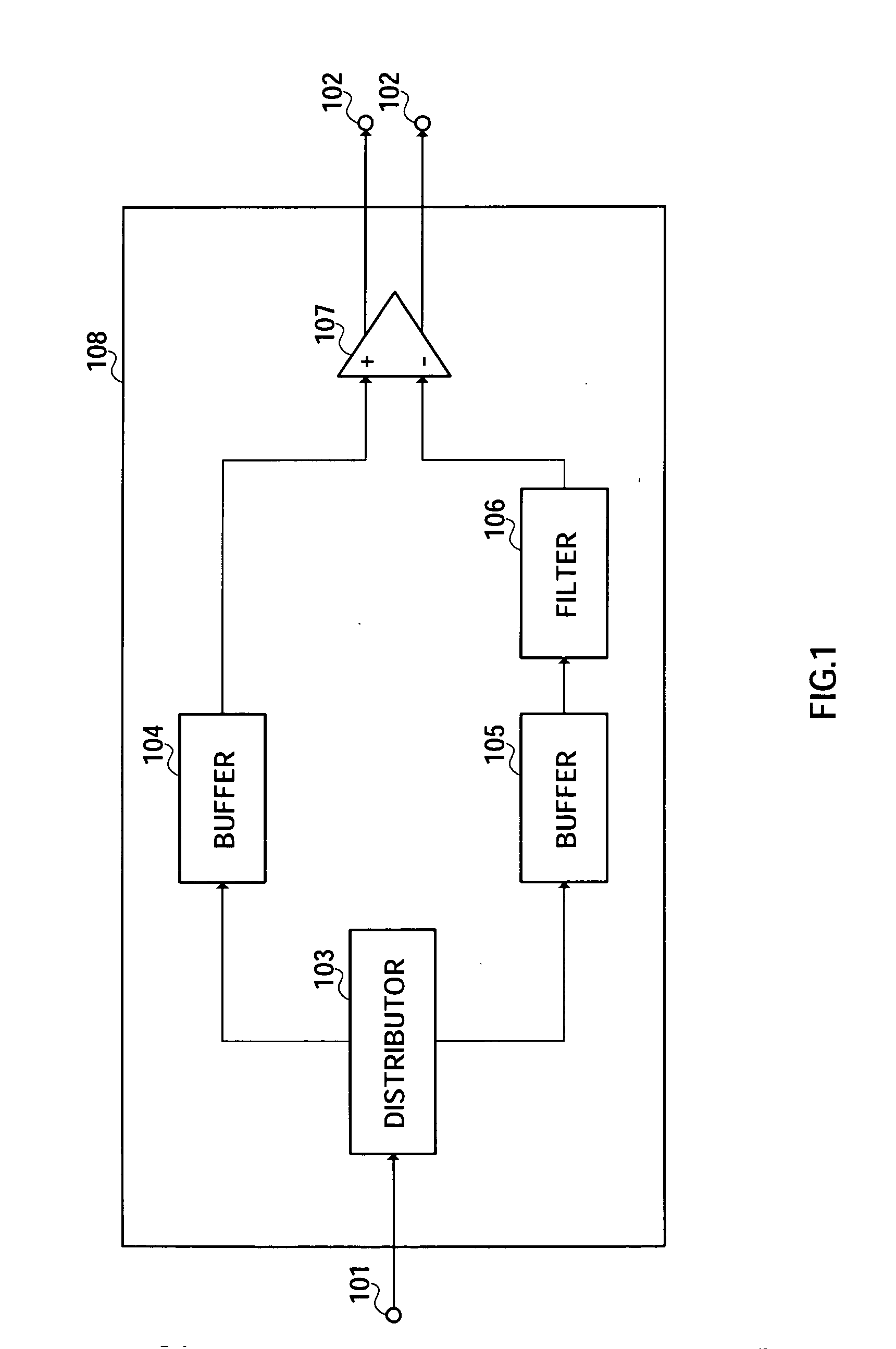
[0025]FIG. 1 is a block diagram showing a configuration of a filter circuit 108 according to Embodiment 1 of the present invention.
[0026] A signal input terminal 101 in FIG. 1 receives an input signal and sends it to a distributor 103. Signal output terminals 102 output output signals from a differential amplifier 107. The distributor 103 distributes a signal in an arbitrary frequency band input from the signal input terminal 101 into two lines of distributed signals of the equal amplitude and equal phase and outputs the respective distributed signals to a buffer 104 and a buffer 105. The buffer 104 suppresses interference between the two lines of distributed signals input from the distributor 103 and outputs the signal to the differential amplifier 107. The buffer 105 suppresses interference between the two lines of distributed signals input from the distributor 103 and outputs the signal to the filter 106. The filter 106 applies a frequency selection to the distributed signal inp...
embodiment 2
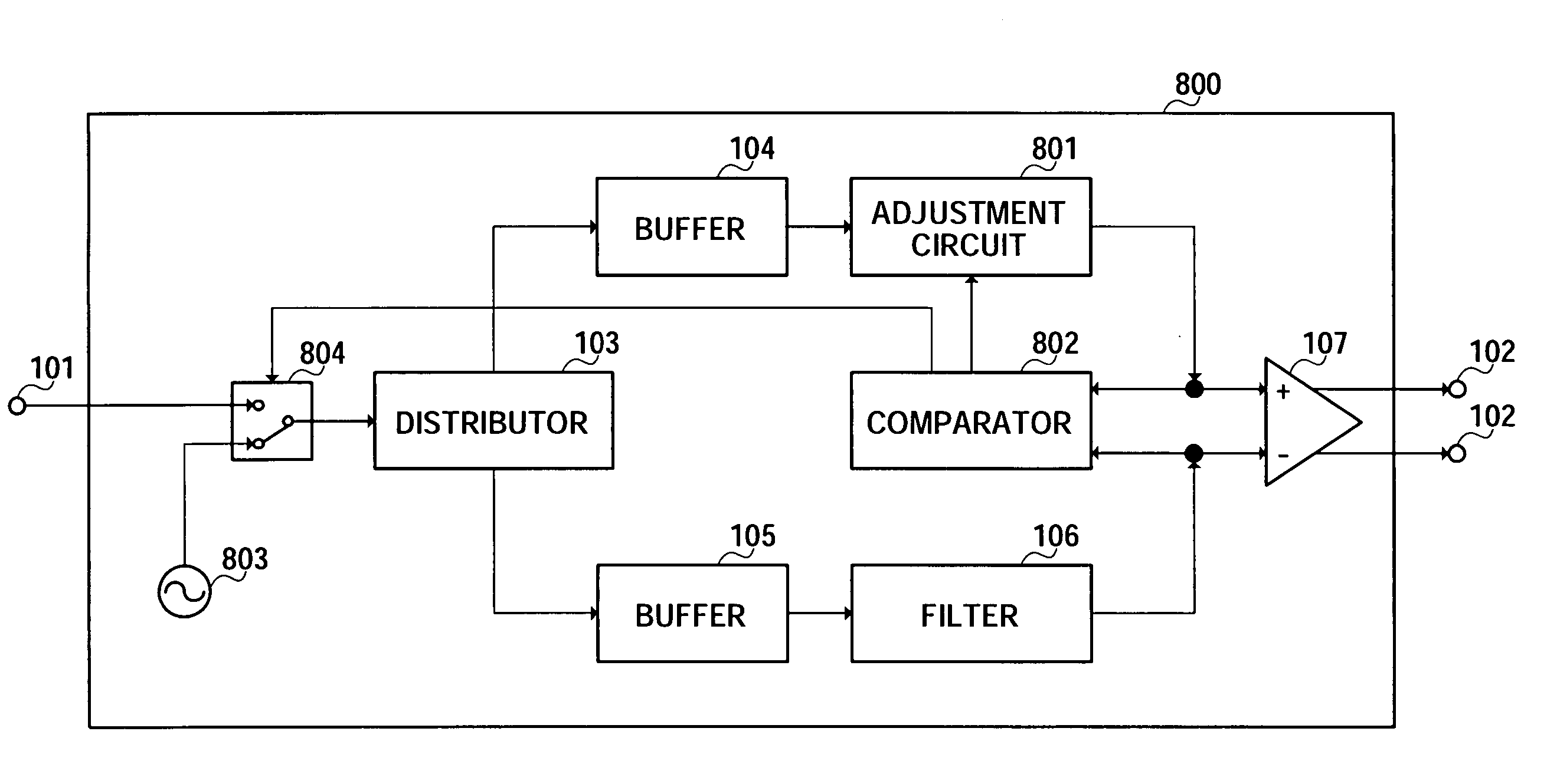
[0036]FIG. 8 is a block diagram showing a configuration of a filter circuit 800 according to Embodiment 2 of the present invention.
[0037] The filter circuit 800 in this Embodiment 2 corresponds to the filter circuit 108 in Embodiment 1 shown in FIG. 1 with an adjustment circuit 801, a comparator 802, a reference signal source 803 and a switch 804 shown in FIG. 8 added. In FIG. 8, the same components as those in FIG. 1 are assigned the same reference numerals and explanations thereof will be omitted.
[0038] In FIG. 8, when the adjustment circuit 801 operates as a calibration circuit, it gives a distributed signal input from the buffer 104 a phase rotation or amplitude attenuation equivalent to an amount of phase rotation or amount of amplitude attenuation which the filter 106 gives to a signal in the pass band and outputs the resultant signal to the comparator 802 and differential amplifier 107. Furthermore, when the adjustment circuit 801 does not operate as a calibration circuit, ...
embodiment 3
[0054]FIG. 9 is a block diagram showing a configuration of a filter circuit 900 according to Embodiment 3 of the present invention.
[0055] The filter circuit 900 according to this Embodiment 3 corresponds to the filter circuit 800 according to Embodiment 2 shown in FIG. 8 with a selector 903 added, the filter 106 replaced by a filter 901 and the adjustment circuit 801 replaced by an adjustment circuit 902 as shown in FIG. 9. In FIG. 9, the same components as those in FIG. 1 and FIG. 8 are assigned the same reference numerals and explanations thereof will be omitted.
[0056] In FIG. 9, the filter 901 has a band-reject type configuration made up of an inductor and a capacitance and makes the rejection band variable by making the inductor value or capacitance value variable. That is, the filter 901 rejects passage of some frequency components in a predetermined communication band and allows only predetermined frequency components to pass. Then, the filter 901 outputs the frequency compo...
PUM
 Abstract
Description
Claims
Application Information
 - R&D Engineer
- R&D Manager
- IP Professional
- Industry Leading Data Capabilities
- Powerful AI technology
- Patent DNA Extraction
Browse by: Latest US Patents, China's latest patents, Technical Efficacy Thesaurus, Application Domain, Technology Topic, Popular Technical Reports.
© 2024 PatSnap. All rights reserved.Legal|Privacy policy|Modern Slavery Act Transparency Statement|Sitemap|About US| Contact US: help@patsnap.com