Method of improving the wafer to wafer uniformity and defectivity of a deposited dielectric film

a dielectric film and defectivity technology, applied in the field of pecvd-enhanced chemical vapor deposition system to deposit thin films, can solve the problems of reducing device yield, material build-up on the reactor walls may also affect the performance and repeatability of the deposition process, adversely affecting the properties of the material being deposited, etc., and achieve the effect of enhancing chemical vapor deposition

a dielectric film and defectivity technology, applied in the field of pecvd-enhanced chemical vapor deposition system to deposit thin films, can solve the problems of reducing device yield, material build-up on the reactor walls may also affect the performance and repeatability of the deposition process, adversely affecting the properties of the material being deposited, etc., and achieve the effect of enhancing chemical vapor deposition

US20050221020A1Inactive Publication Date: 2005-10-06TOKYO ELECTRON LTD

Image

  • Method of improving the wafer to wafer uniformity and defectivity of a deposited dielectric film
  • Method of improving the wafer to wafer uniformity and defectivity of a deposited dielectric film
  • Method of improving the wafer to wafer uniformity and defectivity of a deposited dielectric film

Examples


Embodiment Construction

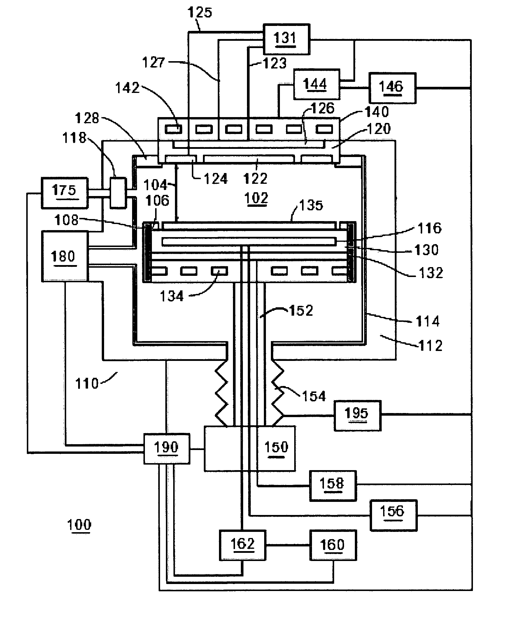
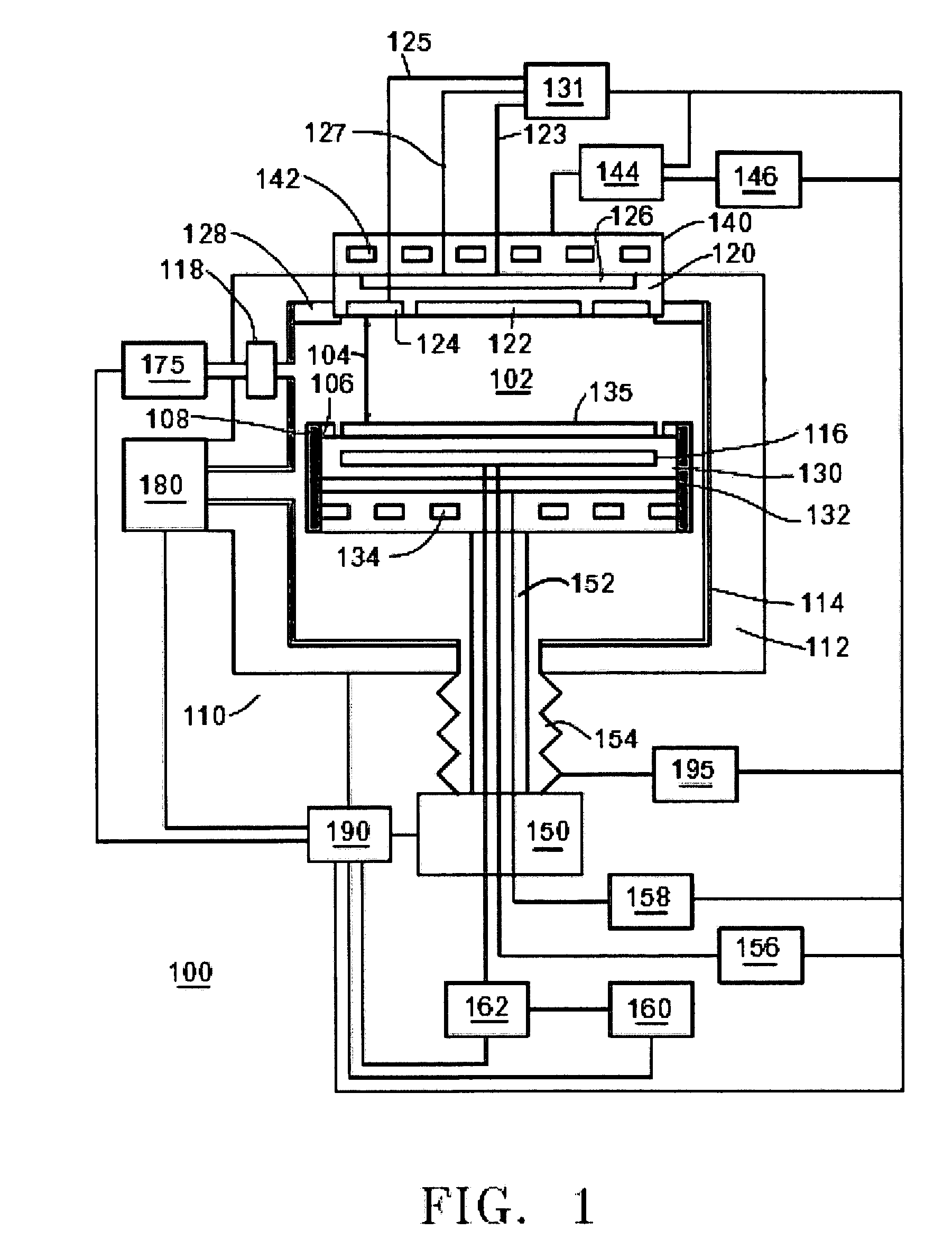
[0019]FIG. 1 illustrates a simplified block diagram for a PECVD system in accordance with an embodiment of the invention. In the illustrated embodiment, PECVD system 100 comprises processing chamber 110, upper electrode 140 as part of a capacitively coupled plasma source, shower plate assembly 120, substrate holder 130 for supporting substrate 135, pressure control system 180, and controller 190.

[0020] In one embodiment, PECVD system 100 can comprise a remote plasma system 175 that can be coupled to the processing chamber 110 using a valve 178. In another embodiment, a remote plasma system and valve are not required. The remote plasma system 175 can be used for chamber cleaning.

[0021] In one embodiment, PECVD system 100 can comprise a pressure control system 180 that can be coupled to the processing chamber 110. For example, the pressure control system 180 can comprise a throttle valve (not shown) and a turbomolecular pump (TMP) (not shown) and can provide a controlled pressure in...


PUM

PropertyMeasurementUnit
Temperatureaaaaaaaaaa
Pressureaaaaaaaaaa

Abstract

A method and apparatus are included that provide an improved deposition process for a Tunable Etch Resistant ARC (TERA) layer with improved wafer to wafer uniformity and reduced particle contamination. More specifically, the processing chamber is seasoned to reduce the number of contaminant particles generated in the chamber during the deposition of the TERA layer and improve wafer to wafer uniformity. The apparatus includes a chamber having an upper electrode at least one RF source, a substrate holder, and a showerhead for providing multiple precursors and process gasses.

Description

CROSS-REFERENCE TO RELATED APPLICATIONS [0001] This application is related to co-pending U.S. patent application Ser. No. 10 / 644,958, entitled “Method and Apparatus For Depositing Materials With Tunable Optical Properties And Etching Characteristics”, filed on Aug. 21, 2003; co-pending U.S. patent application Ser. No. 10 / 702,048, entitled “Method for Improving Photoresist Film Profile”, filed on Nov. 6, 2003; and co-pending U.S. patent application Ser. No. 10 / 702,043, entitled “Method of Improving Post-Develop Photoresist Profile on a Deposited Dielectric Film”, filed on Nov. 6, 2003. The entire contents of these applications are herein incorporated by reference in their entirety.FIELD OF THE INVENTION [0002] The invention relates to using a plasma-enhanced chemical vapor deposition (PECVD) system to deposit thin-film, and more specifically, to depositing films having improved wafer to wafer uniformity and reduced contaminants. BACKGROUND OF THE INVENTION [0003] Integrated circuit a...

Claims


Application Information

Patent Timeline
06 Oct 2005
Publication
US20050221020A1
IPC
H01L21/314; H01J37/32; C23C16/44; H01L21/312
CPC
C23C16/4404; C23C16/4405; H01J37/32862; H01L21/02164; H01L21/02167; H01L21/02211; H01L21/02274; H01L21/3122
Inventors
FUKIAGE, NORIAKI