Lithographic apparatus, device manufacturing method and device manufactured thereby

a technology of lithographic apparatus and manufacturing method, which is applied in the field of lithographic apparatus, a device manufacturing method and a device manufactured thereby, can solve the problems of chip manufacturer, critical dimension (cd), and yield decline, and achieve uniform width and better correction of critical dimension variation

Inactive Publication Date: 2005-10-13
ASML NETHERLANDS BV
View PDF18 Cites 10 Cited by
  • Summary
  • Abstract
  • Description
  • Claims
  • Application Information

AI Technical Summary

Benefits of technology

[0015] Irradiating the annular edge region of the substrate with the beam of compensating radiation, prior to projecting the patterned beam of radiation on to the substrate, means that a layer of photoresist present on the whole exposed surface of the substrate has extra energy applied to it in this edge region, compared with the rest of the substrate which is only irradiated with the subsequently projected patterned beam. Where the pattern projected on to the edge region of the substrate comprises a set of lines of uniform width, this results in a set of lines of non-uniform width on the substrate once the layer of resist on the substrate has been developed, but following a subsequent etch step to etch these developed lines in the substrate the etched lines are found to be more uniform in width. By selecting an appropriate level of intensity, and tilt in the intensity level across the physical sp

Problems solved by technology

One problem encountered in lithography is that the critical dimension (CD), namely the width of a patterned line that can be printed (on the wafer) within design tolerances, varies across the wafer.
This results in a decrease in yield (i.e., less useable chips from each printed wafer) for the chip manufacturer.
However this has the disadvantage that the whole field has an offset applied to it.
This results in an over-correc

Method used


Image

  • Lithographic apparatus, device manufacturing method and device manufactured thereby
  • Lithographic apparatus, device manufacturing method and device manufactured thereby
  • Lithographic apparatus, device manufacturing method and device manufactured thereby

Examples


Embodiment Construction

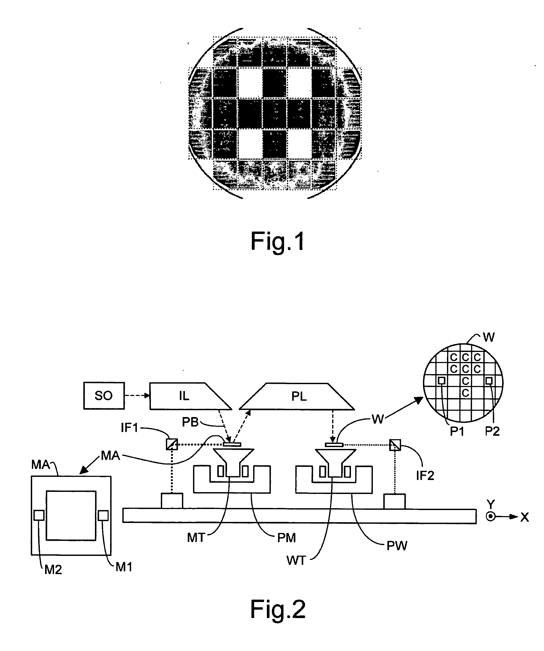
[0038]FIG. 2 schematically depicts a lithographic apparatus according to one particular embodiment of the invention. The apparatus comprises: [0039] an illumination system (illuminator) IL for providing a projection beam PB of radiation (e.g., UV or EUV radiation). [0040] a first support structure (e.g., a mask table) MT for supporting patterning device (e.g., a mask) MA and connected to first positioning means PM for accurately positioning the patterning device with respect to item PL; [0041] a substrate table (e.g., a wafer table) WT for holding a substrate (e.g., a resist-coated wafer) W and connected to second positioning means PW for accurately positioning the substrate with respect to item PL; and [0042] a projection system (e.g., a reflective projection lens) PL for imaging a pattern imparted to the projection beam PB by patterning device MA onto a target portion C (e.g., comprising one or more dies) of the substrate W.

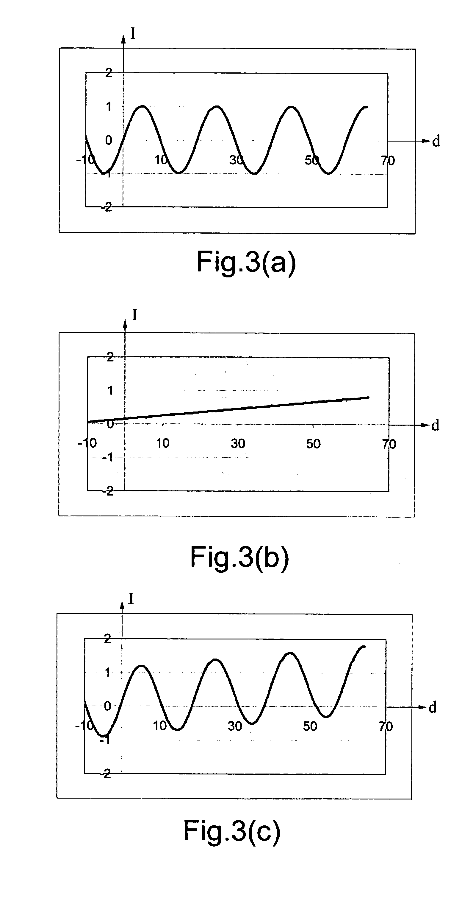
[0043] As here depicted, the apparatus is of a reflectiv...


PUM


Abstract

A device manufacturing method using lithographic apparatus, in which method a patterned beam of radiation is projected on to a target portion of a substrate. Prior to exposing the substrate to the patterned beam of radiation a beam of compensating radiation is irradiated on to a predetermined area of the substrate, the beam of compensating radiation having an intensity which varies across said predetermined area. In the described embodiment the beam of compensating radiation is applied to an annular edge region of the substrate and has an intensity which is tilted across the cross-section of the beam so as to increase or decrease in intensity towards the edge of the substrate. This is done to improve the critical dimension (CD) uniformity across the substrate.

Description

BACKGROUND OF THE INVENTION [0001] 1. Field of the Invention [0002] The present invention relates to a lithographic apparatus, a device manufacturing method and a device manufactured thereby. In particular the invention concerns critical dimension (CD) profile correction in lithography. [0003] 2. Background to the Invention [0004] A lithographic apparatus is a machine that applies a desired pattern onto a target portion of a substrate. Lithographic apparatus can be used, for example, in the manufacture of integrated circuits (ICs). In that circumstance, a patterning device, which is alternatively referred to as a mask or a reticle, may be used to generate a circuit pattern corresponding to an individual layer of the IC, and this pattern can be imaged onto a target portion (e.g., comprising part of, one or several dies) on a substrate (e.g., a silicon wafer) that has a layer of radiation-sensitive material (resist) on it. In general, a single substrate will contain a network of adjac...

Claims


Application Information

Patent Timeline
IPC IPC(8): G03F7/20G03F9/00G21K5/10H01J37/08H01J37/302H01L21/027
CPCG03F7/70425
Inventor HUBERT JACOBUS CARPAIJ, RENEDER LAAN, HANS VAN
Owner ASML NETHERLANDS BV
Why Eureka
Try Eureka