Diamond based blue/UV emission source

a technology of emission source and diamond, which is applied in the direction of basic electric elements, electrical equipment, semiconductor devices, etc., can solve the problems of diamond having some challenges, and achieve the effects of low cost, high reliability and small siz

Inactive Publication Date: 2005-10-13
INPHOT
View PDF0 Cites 14 Cited by
  • Summary
  • Abstract
  • Description
  • Claims
  • Application Information

AI Technical Summary

Benefits of technology

[0020] An object of the present invention is to provide a light emitting diode that can produce frequencies in the ultraviolet and blue portion of the electromagnetic spectrum and that can be incorporated into related devices and equipment, including devices that use phosphors in combination with the LED to produce white light.
[0025] Advantages of the present invention include low cost, high reliability, small size, light weight, and improved heat dissipation.

Problems solved by technology

However, diamond has some challenges as far as the impurity doping and making ohmic contacts is concerned.

Method used


Image

  • Diamond based blue/UV emission source
  • Diamond based blue/UV emission source
  • Diamond based blue/UV emission source

Examples


Embodiment Construction

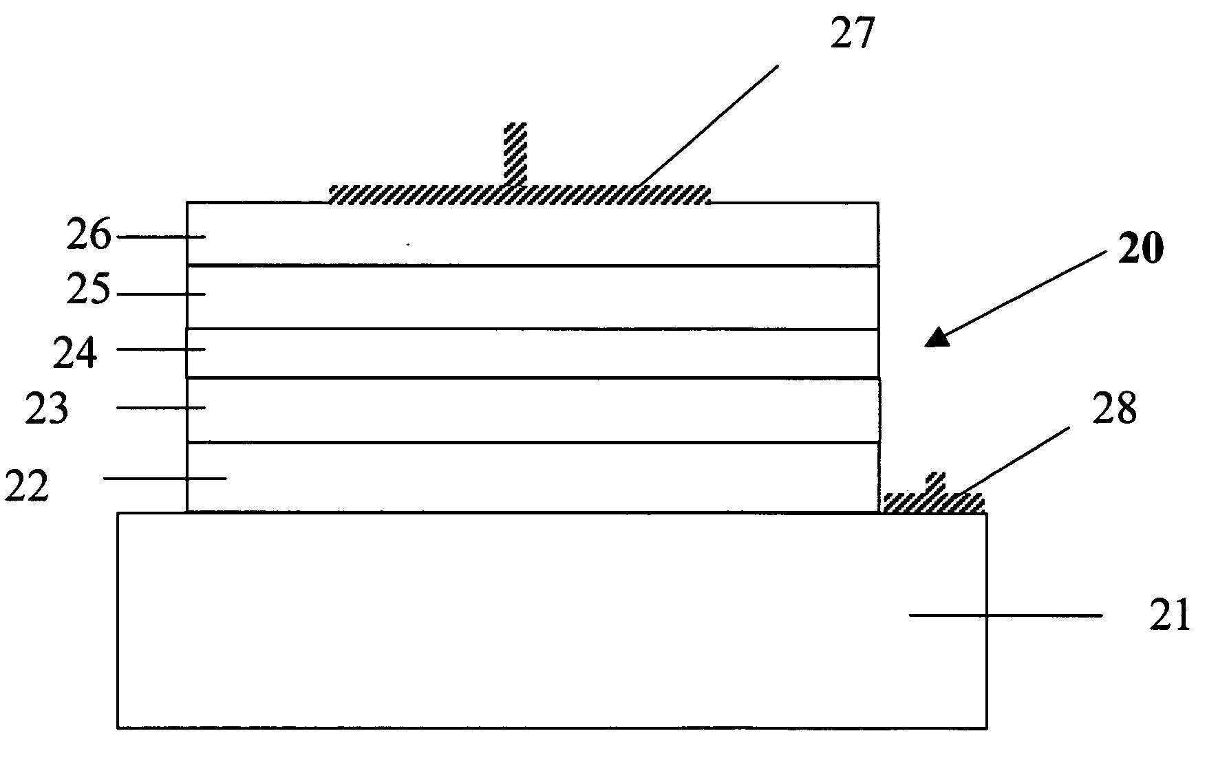
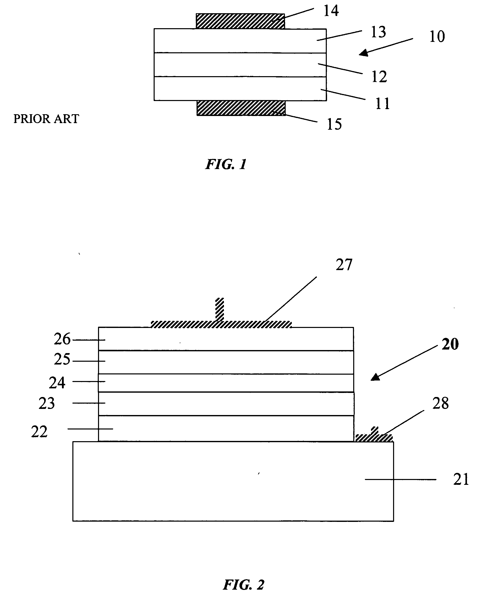
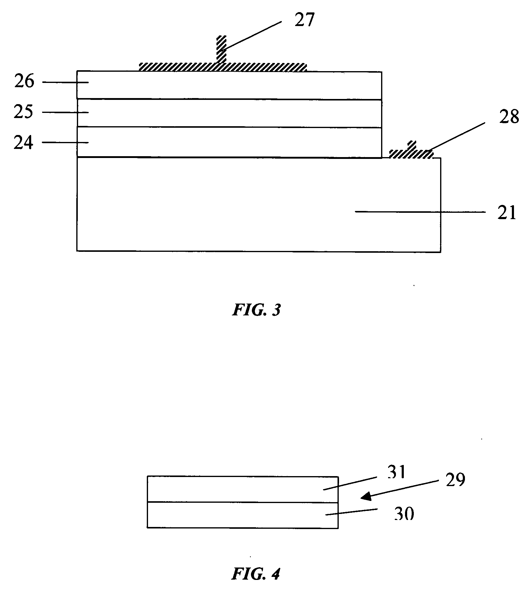
[0026] Referring to FIG. 1, a schematic cross sectional diagram of a simple conventional LED in the prior art is shown. The LED 10 is formed of a substrate 11, and then respective n and p-type epitaxial layers 12 and 13 that form the p-n junction. Ohmic contacts 14 and 15 complete the device in situations where the substrate 11 is conductive. In a device using silicon carbide, the substrate 11 is typically n-type as is the first epitaxial layer 12. The top epitaxial layer 13 is p-type. One of the advantages of silicon carbide as a substrate is its capability of being conductively doped to thus permit the vertical orientation of the device illustrated in FIG. 1. As used in this art, the term “vertical” indicates that the ohmic contacts 14 and 15 are placed at opposite ends of the device so that current can flow through the device in end-to-end fashion rather than laterally, as in LED's that incorporate non-conductive substrates such as sapphire. In its simplest operation, when curren...


PUM

PropertyMeasurementUnit
thicknessaaaaaaaaaa
thicknessaaaaaaaaaa
peak wavelengthaaaaaaaaaa

Abstract

A diamond based Blue / UV light emitting source is disclosed. The source includes a diamond substrate having a first conductivity type, a first aluminum gallium nitride layer above the diamond substrate having the same conductivity type as the substrate, a bulk or a quantum well structure on the AlGaN layer formed of a plurality of repeating sets of alternating layers selected from among GaN, InGaN, and AlInGaN, a second AlGaN layer on the quantum well or the bulk active layer having the opposite conductivity type as the first AlGaN layer, a contact structure on the second AlGaN layer having the opposite conductivity type from the substrate and the first AlGaN layer, an ohmic contact to the diamond substrate, and an ohmic contact to the contact structure.

Description

CROSS REFERENCE TO RELATED APPLICATIONS [0001] This application claims benefit under 35 U.S.C. 119(e) from U.S. Provisional Application No. 60 / 298,835 filed on Mar. 31, 2003.FEDERALLY SPONSORED RESEARCH OR DEVELOPMENT [0002] None. BACKGROUND OF THE INVENTION [0003] 1. Field of the Invention [0004] The present invention relates to light emitting diodes (LEDs) and in particular relates to a light emitting diode formed from diamond substrate and Group III nitrides that emit in the blue and ultraviolet (UV) portion of the electromagnetic spectrum. [0005] 2. Description of the Related Art [0006] A light emitting diode is formed of one or more semiconductor materials that includes at least one p-n junction (the diode) and which emits light (photons) of a particular color when current passes (is injected) through the device. [0007] Because light emitting diodes are formed from semiconductor materials, they represent one group of “solid state” devices; i.e., those electrical or electronic d...

Claims


Application Information

Patent Timeline
Patent Type & Authority Applications(United States)
IPC IPC(8): H01L31/109H01L33/00H01L33/06H01L33/32
CPCH01L33/007H01L33/06H01L33/32
Inventor LINGA, KRISHNAPANAHER, RANJIT
Owner INPHOT
Why Eureka
Try Eureka