Solid-state imaging device, method for driving dolid-state imaging device, imaging method, and imager

a technology of solid-state imaging and drive method, which is applied in the direction of color television, television system, radio control device, etc., can solve the problems of sensitivity decline, unavoidable increase in read-out time, and decrease in the area of the sensor portion per one pixel, so as to improve clock frequency and sensitivity

Inactive Publication Date: 2005-10-13
SONY CORP
View PDF6 Cites 38 Cited by
  • Summary
  • Abstract
  • Description
  • Claims
  • Application Information

AI Technical Summary

Benefits of technology

[0021] The present invention aims to provide a CCD solid state image sensor in which both the clock frequency and the sensitivity can be improved, a method for driving the CCD solid state image sensor, and an image pick-up method and an image pick-up device which use the CCD solid state image sensor.

Problems solved by technology

However, the read-out time unavoidably increases when the number of pixels is increased.
Further, an increase in the number of pixels in the same optical size causes a problem that the area of the sensor portion per one pixel decreases, consequently which causes a problem of the decline of sensitivity.
A limit on this clock frequency and the sensitivity decline per one pixel are the limitation factors for the increase of the pixel numbers in the CCD solid state image sensor which is the mainstream of the solid state image sensor of late.
However, since the electric-charge detection unit in which a signal electric-charge is converted into the pixel signal is divided into a plurality of portions, the density unevenness occurs in the signal level which is output by each block and the seam portion between the blocks becomes discontinuous due to the difference of the conversion gain in the divided electric-charge detection units.
Therefore, the decline in sensitivity caused by the high density pixels may not be compensated with signal correction.
In this case, the density unevenness in the electric-charge detection unit caused by the difference in the conversion gain becomes invisible on the picture due to comparatively high frequency, which is not a problem; however, the reset dispersion among the electric-charge detection units becomes a problem.
However, though the number of CDS circuits decreases in the first method, the processing frequency in the CDS circuit portion is equal to the clock frequency of the horizontal CCD, which becomes a problem with respect to the high density pixels.
Providing the selective gate between the vertical CCD and the electric-charge detection unit is possible when considering the “scanning read-out method” about an equivalent circuit as shown in FIG. 19A; however, wiring of a selection wire to the read-out gate becomes a problem when the actual pattern is considered.
Patterning may be considered to perform on the floating-diffusion FD; however, a problem of noise occurrence is newly caused.
As described above, a problem of sensitivity decline and the decrease in the clock frequency of the horizontal CCD caused by increasing the pixel density remains unsolved in the conventional CCD solid state image sensor.

Method used


Image

  • Solid-state imaging device, method for driving dolid-state imaging device, imaging method, and imager
  • Solid-state imaging device, method for driving dolid-state imaging device, imaging method, and imager
  • Solid-state imaging device, method for driving dolid-state imaging device, imaging method, and imager

Examples


first embodiment

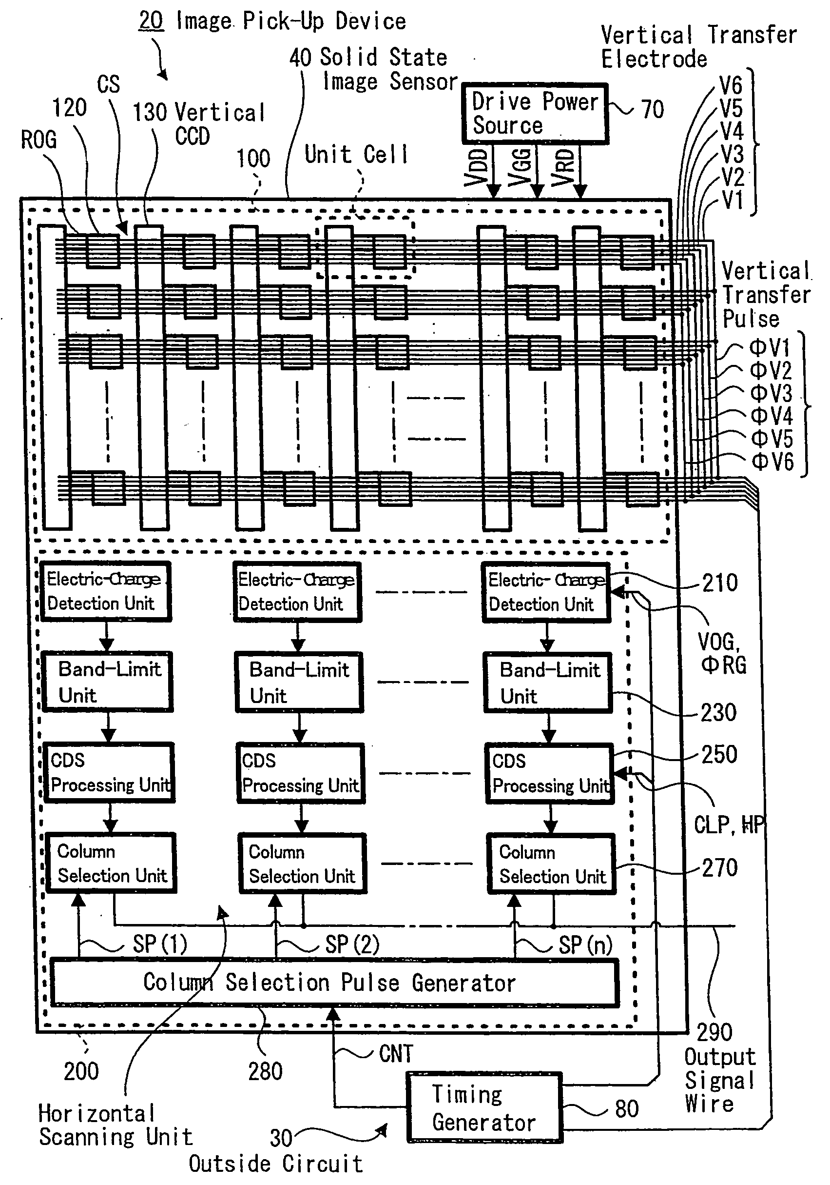
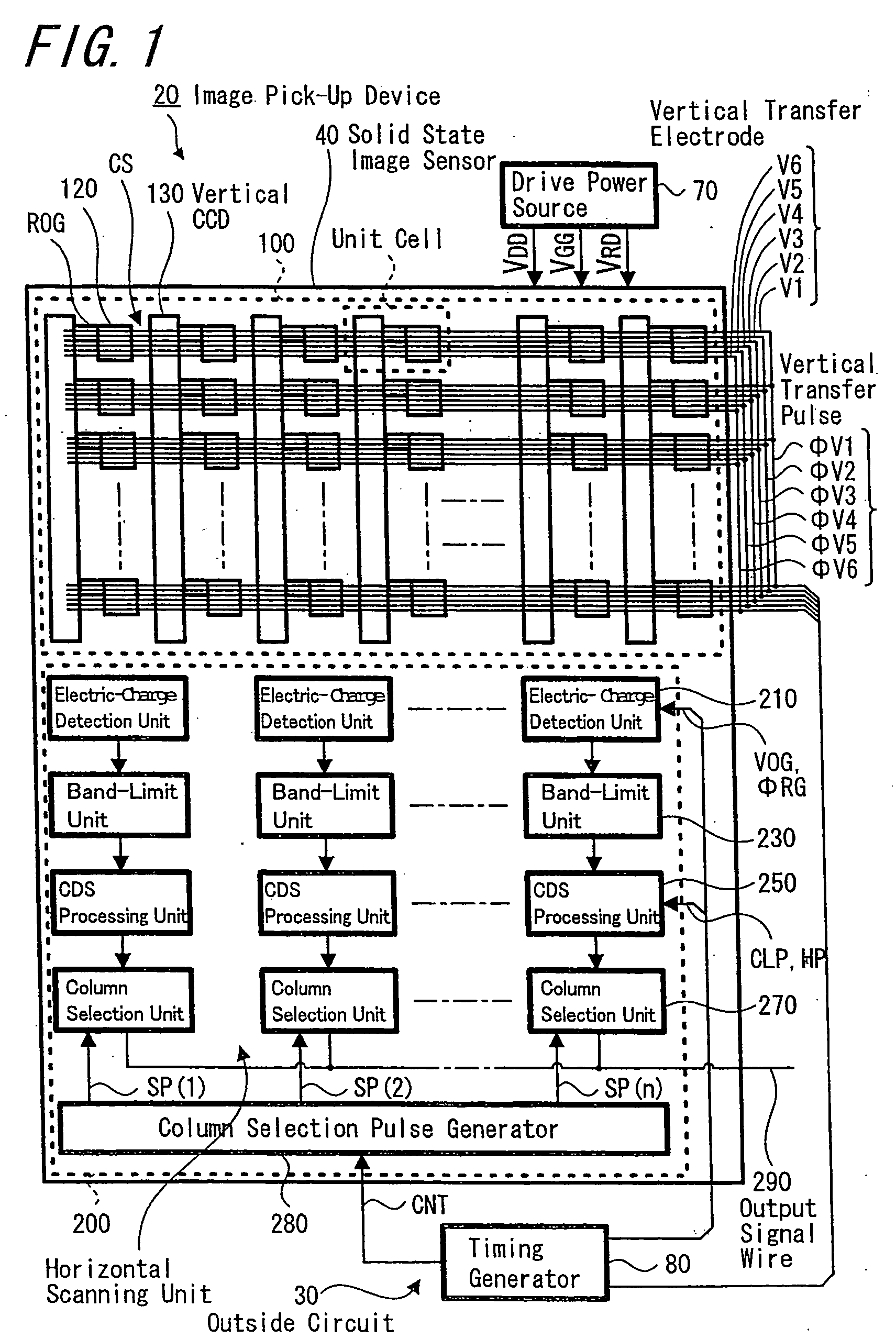
[0066]FIG. 1 is a schematic constitutional view showing an image pick-up device which uses a CCD solid state image sensor according to the present invention and showing the case in which the present invention is applied to a CCD area sensor of an inter-line transfer method.

[0067] As shown in FIG. 1, an image pick-up device 20 includes a CCD solid state image sensor 40 having an image pick-up area 100 and a read-out processing unit 200 arranged on the lower side in the drawing with respect to the image pick-up area 100, and an outside circuit 30 which drives the CCD solid state image sensor 10.

[0068] The outside circuit 30 includes a drive power source 70 which supplies to the CCD solid state image sensor 40 a desired drive voltage such as a drain voltage VDD, a gate voltage VGG or a reset-drain voltage VRD, and a timing generator 80 (TG) which generates various pulse signals such as the vertical transfer pulses φV1 to φV6, a read-out pulse XSG, a selective gate voltage (a fixed vol...

second embodiment

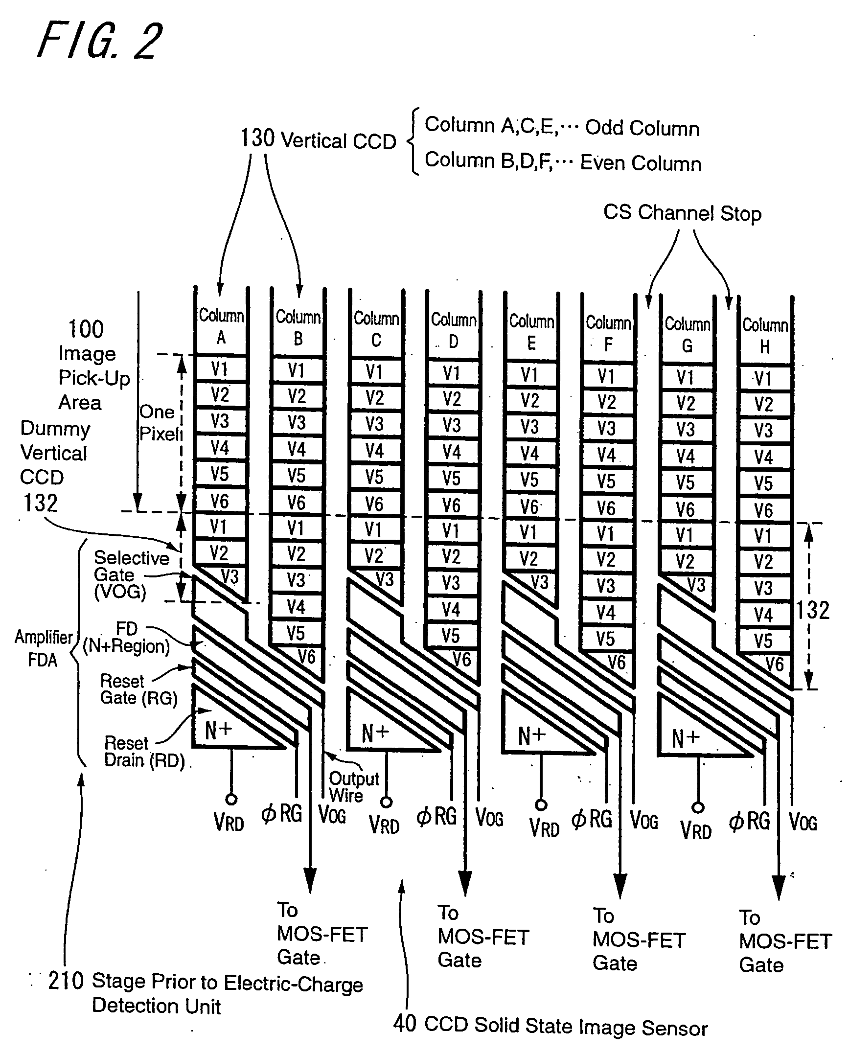
[0166] However, as shown in FIG. 16B, since the fact that the same number of wiring for the selective gate of the vertical CCD 130 is required as that of the vertical CCDs 130 remains unchanged, the ratio of occupying wiring to the area becomes larger than that of the first or the

[0167] The present invention has heretofore been explained using the embodiments; however, the scope of the present invention is not limited to the above-mentioned embodiments. Various changes or improvement can be added to the above embodiments within the range not departing from the spirit of the invention, and embodiments to which such changes or improvement is applied are also included in the scope of this invention.

[0168] Moreover, the invention described in appended claims is not limited by the above-described embodiments, and all the combinations of the characteristics being explained in the embodiments are not necessarily indispensable for the solution means of the invention. In the above-mentioned...


PUM


Abstract

The present invention relates to a CCD solid state image sensor of a scanning read-out type and to a drive method thereof as well as an image pick-up method and the image pick-up device, particularly in which a plurality of vertical CCD columns can be assigned to one electric-charge detection unit with the small number of wiring. In the present invention, adjacent columns of the vertical CCDs are assigned to one electric-charge detection unit. Further, the stages of the voltage transfer between the vertical CCD column and a voltage detection unit is made different; the electrode arrangement is devised; or the drive timing is adjusted. Accordingly, the phase of electric-charge transfer with respect to the plurality of adjacent vertical CCD columns, when the horizontal electric-charge at the same position in the direction of the row obtained by the photo-conductive units is made to reach the electric-charge detection unit, becomes different.

Description

TECHNICAL FIELD [0001] The present invention relates to a solid state image sensor, a drive method of the solid state image sensor, an image pick-up method and an image pick-up device. BACKGROUND ART [0002] Conventionally, CCD (charge couple device) has widely been used as an electric-charge transfer unit of an image pick-up device. When the CCD is used for an image pick-up device, approximately the same number of vertical CCDs as the number of horizontal pixels and one horizontal CCD are arranged, and electric-charge is transferred from the photo-electric converter that is arranged in each pixel to the vertical CCD, the horizontal CCD and the output unit. [0003] Lately, due to the demand for the miniaturization and the high resolution of an image in a camcorder and others, increasing the number of pixels in the same optical size is attempted so that the picture resolution of an image pick-up device is improved. However, the read-out time unavoidably increases when the number of pix...

Claims


Application Information

Patent Timeline
Patent Type & Authority Applications(United States)
IPC IPC(8): H04N5/335H04N5/378H04N5/341H04N5/363H04N5/3728H04N5/376H04N5/369H01L29/768H01L27/148
CPCH01L27/14831H01L29/76816H04N5/335H04N5/378H04N5/3728H04N25/00H04N25/73H04N25/75H04N25/40H04N25/71
Inventor TOYAMA, TAKAYUKI
Owner SONY CORP
Why Eureka
Try Eureka