Circuit device and method of manufacturing the circuit device

a circuit device and manufacturing method technology, applied in the field of circuit devices, can solve the problems of increasing the difficulty of obtaining a high q characteristic, reducing the joint strength, and difficult to keep the high q characteristic, so as to reduce the electric resistance of the wiring pattern, increase the production steps, and the effect of low price devi

Inactive Publication Date: 2005-10-13
TDK CORPARATION
View PDF8 Cites 19 Cited by
  • Summary
  • Abstract
  • Description
  • Claims
  • Application Information

AI Technical Summary

Benefits of technology

[0018] Under such circumstance, a first object of the invention is to provide a circuit device that has connection bumps on a surface of a substrate and laminated layer formation of the same metallic film as UBM in the UBM processing, so that the l...

Problems solved by technology

As a result, characteristic of the circuit device might be influenced by the decrease in joint strength and the problem is caused in reliability.
Consequently, the generated voids might cause the decrease in joint strength.
When a high density device formation is requested to the IC substrate, the coil shapes inevitably becoming small and the accumulation space of the magnetic energy of the coil is small, and it becomes difficult more and mo...

Method used


Image

  • Circuit device and method of manufacturing the circuit device
  • Circuit device and method of manufacturing the circuit device
  • Circuit device and method of manufacturing the circuit device

Examples


Embodiment Construction

[0034] Embodiments of the invention as to a circuit device and manufacturing method of the same will be described below with reference to the drawings.

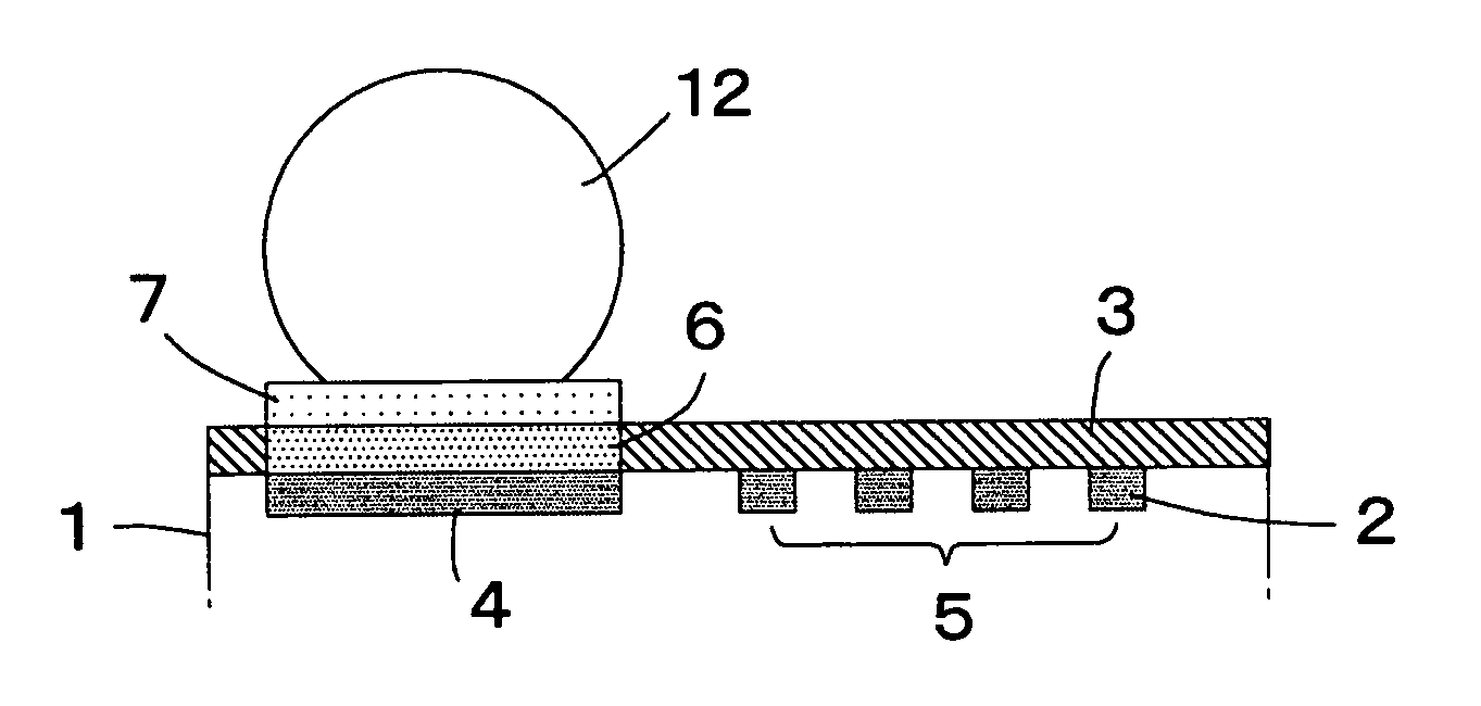
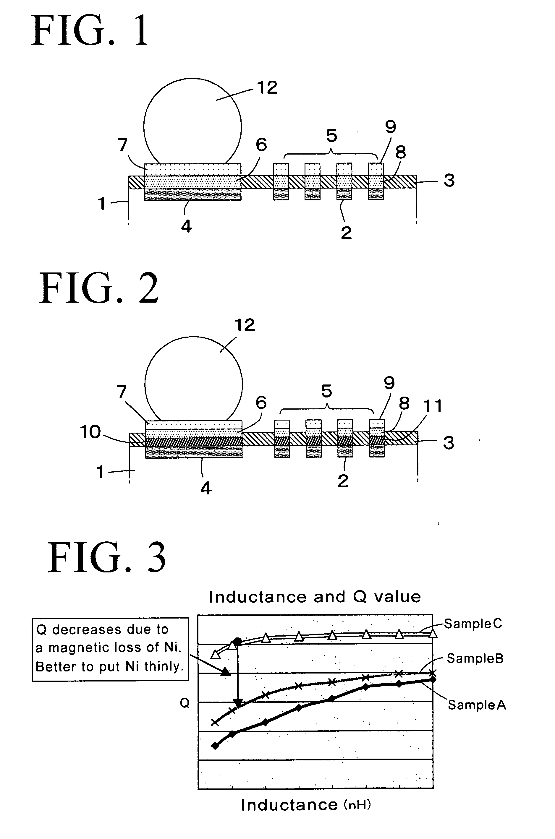
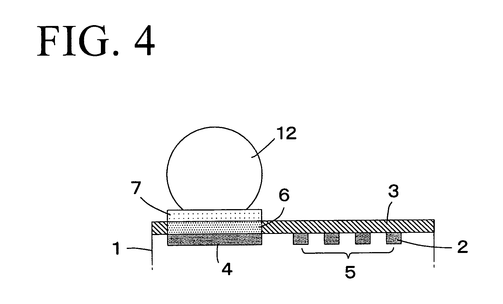
[0035]FIG. 1 is a cross-sectional view of a first embodiment to explain a structure and a production process of a circuit device that contains a high frequency thin film coil. The same numerals are fixed to common members in the prior art (refer to FIG. 4) and FIG. 1, and the explanations thereof are omitted. The different point of the device of the first embodiment from the prior art (refer to FIG. 4) is that a passivation film 3 is formed on a surface of a substrate 1 on the condition that a part of (or all of) the wiring pattern 2 forming a high frequency coil 5 and an electrode pad pattern 4 of an Al film as a putting part of a metallic connection bump 12 are exposed by an exposure development processing method for instance by photo lithography or the like. The bump 12 is provided through which an electrical connection is achieve...


PUM


Abstract

A circuit device comprises at least one under bump metal formed on a surface of a substrate and a connection bump provided on the uppermost layer of the under bump metal. At least one laminated metallic film is formed on part of or all of wiring pattern formed on the surface of the substrate, so that the laminated metallic film formed is consisted of the same material and also the same thickness as the under bump metal.

Description

BACKGROUND OF THE INVENTION [0001] 1. Field of the Invention [0002] The invention relates to a circuit device and a manufacturing method of the same, used for transmitting and receiving wireless telecommunications equipments such as a wireless LAN, ETC, and cellular phones, etc., and especially to a semiconductor integrated circuit device and a manufacturing method of the same which contains a high frequency thin film coil or the like. [0003] 2. Description of the Prior Art [0004] As for the wireless equipments such as the wireless LAN, ETC, and cellular phones, etc. downsizing comes to be demanded by recent market trend more and more. It has been taken widely in recent years that an industrial method uses metallic bumps for electrical connections provided on a Si-IC substrate (bare IC chip) of the equipments and connects the Si-IC substrate on a surface of other substrate through the bumps by flip chip bonding, etc. [0005] By the way, it has been made an universal method of using A...

Claims


Application Information

Patent Timeline
IPC IPC(8): H01L23/485H01L21/60H01L23/522
CPCH01L23/5227H01L2224/0401H01L2224/13099H01L2924/01004H01L2924/01005H01L2924/01006H01L2924/01013H01L2924/01014H01L2924/01022H01L2924/01028H01L2924/01029H01L2924/01032H01L2924/01033H01L2924/01046H01L2924/01074H01L2924/01078H01L2924/01079H01L2924/01082H01L2924/014H01L2924/14H01L2924/30105H01L2924/30107H01L2924/3011H01L2924/01024H01L2924/0002H01L2224/05552H01L2224/0558H01L24/03H01L24/05H01L24/13H01L2224/0345H01L2224/03462H01L2224/03464H01L2224/05124H01L2224/05567H01L2224/05582H01L2224/05644H01L2224/05647H01L2224/05655H01L2224/05666H01L2224/05669H01L2224/05671H01L2224/05684H01L2224/13144H01L2224/05568H01L2224/05583
Inventor DOMON, TAKAAKINAGATSUKA, TOSHIYUKIYASUI, TSUTOMUKONDO, RYOICHI
Owner TDK CORPARATION
Why Eureka
Try Eureka