Extension of fatigue life for C4 solder ball to chip connection

a fatigue life and solder ball technology, applied in the direction of printed circuit assembling, printed circuit manufacturing, basic electric elements, etc., can solve the problems of thermally induced strain and electrical failure of the solder ball that couples a semiconductor chip to an organic chip carrier, and achieve the effect of reducing thermally induced strain

Inactive Publication Date: 2005-10-13
GLOBALFOUNDRIES INC
View PDF20 Cites 20 Cited by
  • Summary
  • Abstract
  • Description
  • Claims
  • Application Information

AI Technical Summary

Benefits of technology

[0021] The present invention reduces thermally induced strain that occurs in a solder ball during thermal cycling, wherein the solder ball couples a semiconductor chip to an organic chip carrier.

Problems solved by technology

A solder ball that couples a semiconductor chip to an organic chip carrier is subject to thermally induced strain during thermal cycling.
The thermally induced strain inevitably causes damage to the solder leading to cracking and electrical failure if sufficient cycles occur.

Method used


Image

  • Extension of fatigue life for C4 solder ball to chip connection
  • Extension of fatigue life for C4 solder ball to chip connection
  • Extension of fatigue life for C4 solder ball to chip connection

Examples


Embodiment Construction

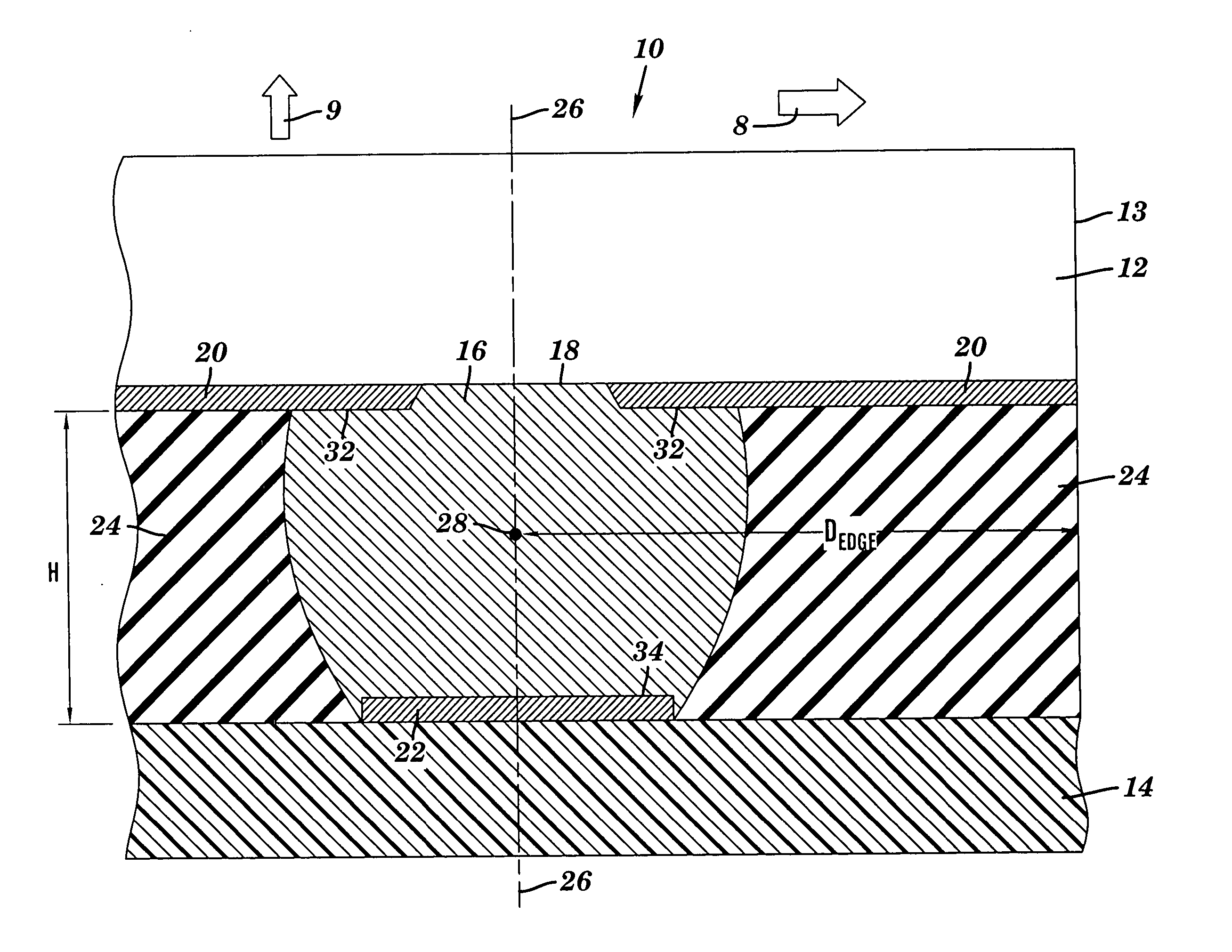
[0026]FIG. 1 illustrates a front cross-sectional view of an electronic structure 10, in accordance with embodiments of the present invention. The electronic structure 10 includes a semiconductor substrate 12 coupled to an organic substrate 14 by a solder member 16. The solder member 16 is mechanically and electrically coupled to an electrically conductive pad 20 on the semiconductor substrate 12. The solder member 16 is likewise mechanically and electrically coupled to an electrically conductive pad 22 on the organic substrate 14.

[0027] The semiconductor substrate 12 may include, inter alia, a semiconductor chip (e.g., a silicon chip or a germanium chip). The semiconductor substrate 12 may have a coefficient of thermal expansion (CT-E) of about 3 ppm / ° C., wherein ppm stands for parts per million.

[0028] The organic substrate 14 includes, inter alia, an organic material such as an epoxy, a polyimide, a polytetrafluoroethylene (PTFE), glass cloth, copper-invar-copper or other reinfo...


PUM

PropertyMeasurementUnit
elastic modulusaaaaaaaaaa
distanceaaaaaaaaaa
distanceaaaaaaaaaa

Abstract

A method and structure for coupling a semiconductor substrate (e.g., a semiconductor chip) to an organic substrate (e.g., a chip carrier). The coupling interfaces a solder member (e.g., a solder ball) to both a conductive pad on the semiconductor substrate and a conductive pad on the organic substrate. Thermal strains on the solder member during thermal cycling may be reduced by having a surface area of the pad on the semiconductor substrate exceed a surface area of the pad on the organic substrate. Thermal strains on the solder member during thermal cycling may also be reduced by having a distance from a centerline of the solder member to a closest lateral edge of the semiconductor substrate exceed about 0.25 mm.

Description

BACKGROUND OF THE INVENTION [0001] 1. Technical Field [0002] The present invention relates to a method and structure for coupling a semiconductor chip to an organic chip carrier by a solder ball. [0003] 2. Related Art [0004] A solder ball that couples a semiconductor chip to an organic chip carrier is subject to thermally induced strain during thermal cycling. The thermally induced strain inevitably causes damage to the solder leading to cracking and electrical failure if sufficient cycles occur. Thus, a method and structure is needed for reducing the aforementioned thermally induced strain and increasing the fatigue life. SUMMARY OF THE INVENTION [0005] The present invention provides an electronic structure, comprising: [0006] a semiconductor substrate having a first electrically conductive pad thereon; [0007] an organic substrate having a second electrically conductive pad thereon, wherein a surface area of the first pad exceeds a surface area of the second pad; and [0008] a solde...

Claims


Application Information

Patent Timeline
Patent Type & Authority Applications(United States)
IPC IPC(8): H01L21/60H01L23/485H05K3/34
CPCH01L24/10H01L24/81H01L2224/13099H01L2224/13111H01L2224/81801H01L2924/01004H01L2924/01015H01L2924/01029H01L2924/01032H01L2924/01033H01L2924/01057H01L2924/01058H01L2924/01082H01L2924/01322H05K3/3436H01L2924/01005H01L2924/01006H01L2924/01047H01L2924/0105H01L2924/014H01L2924/10253H01L2924/00H01L2924/351H01L24/13H01L2224/13H01L21/60
Inventor BERNIER, WILLIAM E.CAREY, CHARLES F.GRAMATZKI, EBERHARD B.HOMA, THOMAS R.JOHNSON, ERIC A.LANGEVIN, PIERREMEMIS, IRVINGTRAN, SON K.WHITE, ROBERT F.
Owner GLOBALFOUNDRIES INC
Why Eureka
Try Eureka