
Input matching circuit for multiband low noise amplifier

Inactive Publication Date: 2005-10-13
SAMSUNG ELECTRONICS CO LTD +1
View PDF3 Cites 22 Cited by
  • Summary
  • Abstract
  • Description
  • Claims
  • Application Information

AI Technical Summary

Benefits of technology

[0015] It is, therefore, an object of the present invention to provide a dual-band low noise amplifier for minimizing the number of components constituting a circuit without compromising amplification performance of multiband signals.

Problems solved by technology

As a result, a number of expensive external components are required, more space is required to mount such external components, and manufacturing costs increase.
Since there is a trade-off between image rejection and channel selection, double down conversion mixing is required for each path, resulting in increases in complexity and power consumption.
However, the dual-band receiver using a conventional Weaver architecture does not provide sufficient image rejection and requires a large mounting space, causing an increase in manufacturing costs.
Moreover, although the dual-band receiver using a conventional Weaver architecture is smaller than the dual-band receiver of FIG. 1, it consumes much power.
However, performance degradation may occur due to noises caused by the switches and the complexity of controlling the switches and a mounting space is relatively large.
However, a change in the bias current brings about unfavorable changes in a direct current condition, leading to performance degradation.

Method used


Image

  • Input matching circuit for multiband low noise amplifier
  • Input matching circuit for multiband low noise amplifier
  • Input matching circuit for multiband low noise amplifier

Examples


Embodiment Construction

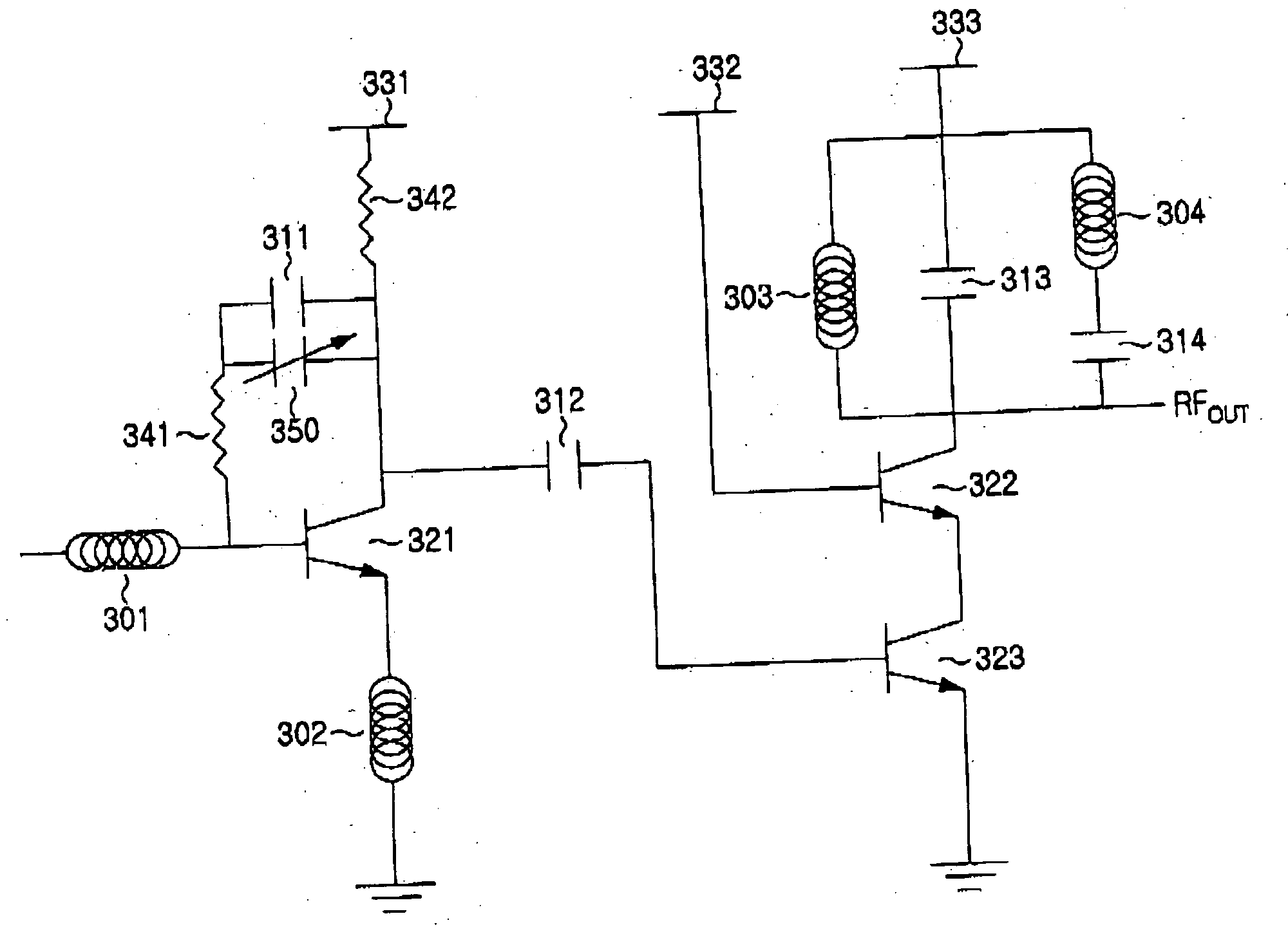
[0022] A multiband low noise amplifier according to a preferred embodiment of the present invention will now be described in detail with reference to the annexed drawings.

[0023]FIG. 3 is a circuit diagram of a multiband low noise amplifier according to a preferred embodiment of the present invention.

[0024] A multiband low noise amplifier according to a preferred embodiment of the present invention includes a first inductor 301, a first resistor 341, a first capacitor 311, a varactor 350, a first power supply 331, a second resistor 342, a first transistor 321, a second inductor 302, a second capacitor 312, a second power supply 332, a third inductor 303, a third power supply 333, a third capacitor 313, a second transistor 322, a third transistor 323, a fourth inductor 304, and a fourth capacitor 314.

[0025] As shown in FIG. 3, the first transistor 321 includes an emitter grounded through the second inductor 302, a collector connected to the first power supply 331 through the second...


PUM


Abstract

Provided is a multiband low noise amplifier including a first transistor, an input matching circuit, and a first capacitor. The first transistor includes a collector electrically connected to a first power supply, a grounded emitter, and a base connected to the other end of a first inductor having one end as an input end of the low noise amplifier. The input matching circuit is connected between the collector and the base of the first transistor. The first capacitor connected to the collector of the first transistior. The input matching circuit includes a varactor. The input matching circuit includes a second capacitor connected to the varactor. The input matching circuit includes a first resistor connected to the varactor. In the multiband low noise amplifier, a varactor having a variable capacitance is installed at an input end, thereby easily performing band switching through bias voltage control by a small amount and minimizing noises that may be caused by a control signal.

Description

PRIORITY [0001] This application claims priority under 35 U.S.C. § 119 to an application entitled “Input Matching Circuit for Multiband Low Noise Amplifier” filed in the United States Patent and Trademark Office on Mar. 24, 2004 and assigned Ser. No. 60 / 555,684, and an application entitled “Input Matching Circuit for Multiband Low Noise Amplifier” filed in the Korean Intellectual Property Office on Dec. 31, 2004 and assigned Serial No. 2004-118153, the contents of both of which are incorporated herein by reference.BACKGROUND OF THE INVENTION [0002] 1. Field of the Invention [0003] The present invention relates generally to a multiband low noise amplifier, and in particular, to an input matching circuit for a multiband low noise amplifier. [0004] 2. Description of the Related Art [0005] In a wireless communication system such as a wireless telephone, a number of electronic components for transceiving signals through a wireless medium are used. For example, a transceiver transmits and...

Claims


Application Information

Patent Timeline
IPC IPC(8): H03F3/191H04B1/40H03F3/68H04B1/18
CPCH03F3/191H03F2200/294H03F2200/372H03F2203/7209H04B1/18H04B1/40
Inventor BHATIA, RAHULWOO, SANG-HYUNBANG, JI-HOONLEE, SEONG-SOOLEE, CHANG-HOLASKAR, JOY
Owner SAMSUNG ELECTRONICS CO LTD
Features
  • Generate Ideas
  • Intellectual Property
  • Life Sciences
  • Materials
  • Tech Scout
  • Unparalleled Data Quality
  • Higher Quality Content
  • 60% Fewer Hallucinations
Learn More