Optical element and processing method for the same

Inactive Publication Date: 2005-10-13
CANON KK
View PDF2 Cites 0 Cited by
  • Summary
  • Abstract
  • Description
  • Claims
  • Application Information

AI Technical Summary

Benefits of technology

[0007] The present invention has been made in view of the problems described above, and has as its object to be able to easily obtain high shape precision and high surface smoothness when an optical element is to be formed by pressing a metal plate.

Problems solved by technology

Therefore, when a formed product such as a concave mirror is to be manufactured by pressing, as the transcribing performance of the press die differs between the rolling direction and the direction perpendicular to the rolling direction, it is difficult to obtain high shape precision.
Also, as the hardness of the material surface is high, it is difficult to sufficiently transcribe the smoothness of the surface of the press die to the surface of the press formed product.
For these reasons, in most metal reflecting optical elements, as seen in above patent references 1 to 3, polishing and mirror-surface processing are performed to ensure the shape precision and surface roughness, however, this results in long processing times.
Then, in the press step, the smoothness of the surface of the press die cannot be sufficiently transcribed to the surface of the press formed product, and surface cracks tend to easily occur, making it difficult to form a free-form surface which is smooth and has a small curvature radius.
According to another method, a commercially available expensive optical aluminum material is used.
However, as the hardness of the material surface is high, the smoothness of the die cannot be sufficiently transcribed, and the resulting surface roughness is as high as 10 nm or more.

Method used


Image

  • Optical element and processing method for the same
  • Optical element and processing method for the same
  • Optical element and processing method for the same

Examples


first embodiment

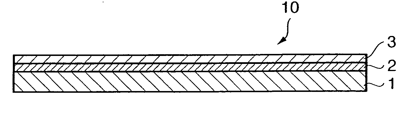
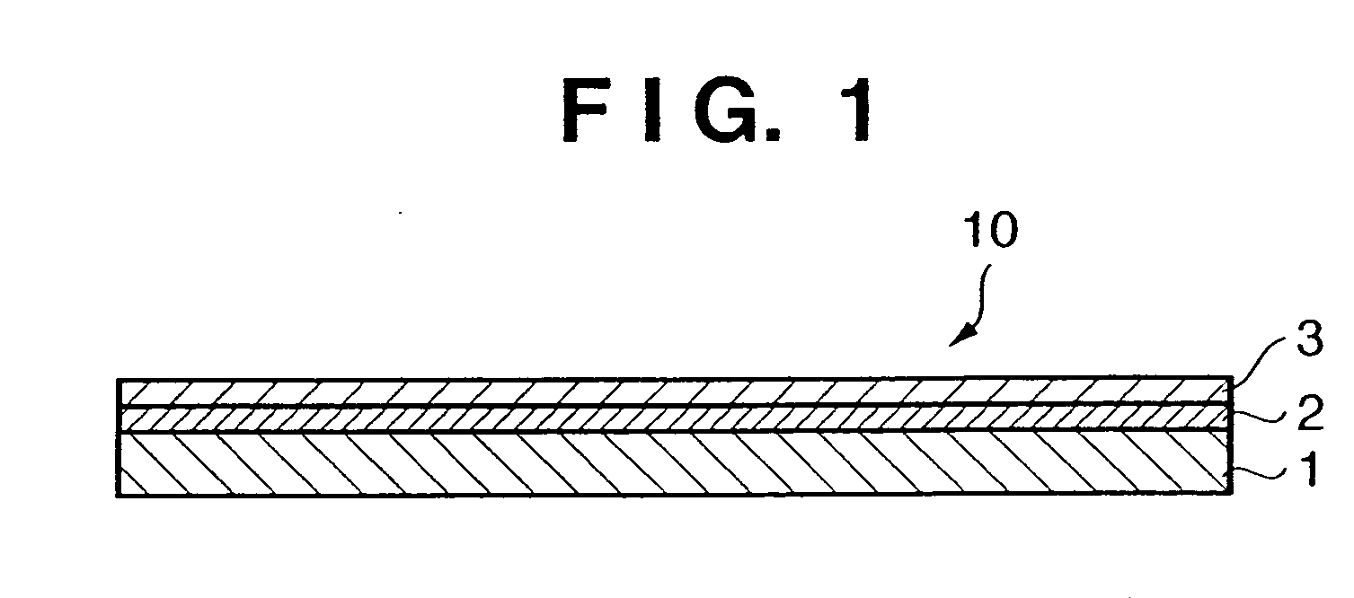
[0028]FIG. 1 is a cross-sectional view showing a state wherein a high-purity metal film 3 is formed on one surface of a plate material 10, i.e., a base material 1, serving as a material to manufacture a curved surface mirror. An undercoat 2 is formed on the surface of the base material 1 to increase the adhesion strength between the base material 1 and high-purity metal film 3.

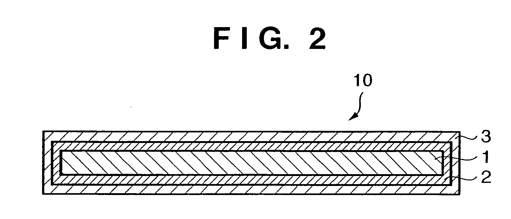
[0029]FIG. 2 is a cross-sectional view showing a state wherein a high-purity metal film 3 is formed on each of the two surfaces of a base material 1 in the same manner as in FIG. 1.

[0030]FIG. 3 is a cross-sectional view of a finished formed product which is manufactured by forming the plate material 10 shown in FIG. 1 with a die.

[0031]FIG. 4 is a cross-sectional view showing a state wherein a reflecting film, a protective film, or a laminated film 4 of a reflecting film and protective film is formed on the optical surface of the finished press formed product shown in FIG. 3.

[0032]FIG. 5 is a cross-sectiona...

second embodiment

[0056] The second embodiment of the present invention will be described.

[0057] The sectional structure of a plate material 10 as a forming material of this embodiment is similar to that of the first embodiment shown in FIGS. 1 to 5.

[0058] First, to transcribe the smoothness of a die which is made very smooth on the nanometer level onto a forming material (plate material 10), at least the surface layer of the plate material 10 serving as the forming material must have a high purity, and each of an initial surface layer (a high-purity metal film 3) and a base material 1 must have a low dislocation density and isotropic structure. Unlike in the patent reference 1, the formed film need not have a spherical texture.

[0059] Generally, between a shearing deformation stress τ and average dislocation density ρ, a relation of τ =τ0+αμb{square root}{square root over ( )}τ (where τ0 and α: constants; μ: modulus of rigidity; and b: Burgers vector) is established. When ρ is large, deformation i...

third embodiment

[0079] The third embodiment of the present invention will be described with reference to the accompanying drawings.

[0080]FIG. 9 is a sectional view showing a plate material 10 serving as a material to manufacture a curved surface mirror. The plate material 10 is obtained by forming a high-purity metal film 3 on one surface of a metal base material 1 by deposition. An undercoat 2 is formed on the surface of the base material 1 to increase the adhesion strength between the base material 1 and high-purity metal film 3. An oxide film 5 which is oxidized by oxygen in the ambient environment during the deposition process is formed on the surface of the high-purity metal film 3. An example of the ambient environment during deposition of the high-purity metal film 3 includes air, an inert gas, a vacuum, and the like. Not only air but also an inert gas, vacuum, or the like contains a small amount of oxygen that oxidizes the surface of the high-purity metal film 3, and accordingly the oxide ...


PUM


Abstract

The object of the present invention is to enable the manufacture of an optical element curved surface mirror with a low surface roughness and high shape precision at a low cost by only forming without employing any one of various types of polishing operations during a manufacturing process. In order to achieve this object, the present invention provides an optical element processing method of forming an optical element by forming a metal base material with a die, and includes a film formation step of forming a metal film on a surface of the metal base material by PVD, CVD, plating, or dipping, and a forming step of forming the metal base material, having the metal film formed on its surface, with the die.

Description

FIELD OF THE INVENTION [0001] The present invention relates to a technique for manufacturing a reflecting optical element by press-forming a metal plate. BACKGROUND OF THE INVENTION [0002] Conventionally, an image system, which uses a reflecting optical element, such as a flight simulator, head-mounted display, projector, and the like, are known. Among these systems, particularly as a proposal of a reflecting optical element material mainly containing a metal material or a reflecting optical element, a reflecting material in which an Al (aluminum) base metal is continuously deposited on the surface of an Al rolled material, as disclosed in Japanese Patent Laid-Open No. 7-243027, is known. Also, a method of manufacturing a curved surface mirror by processing, particularly a stainless steel plate material, which is mirror-surface polished, in accordance with press forming or bulge forming, as disclosed in Japanese Patent Laid-Open No. 8-36222, is known. In addition, a method of obtain...

Claims


Application Information

Patent Timeline
IPC IPC(8): G02B5/10G02B7/182
CPCG02B5/10
Inventor ISHIZUKA, KEIICHI
Owner CANON KK
Why Eureka
Try Eureka