Image forming apparatus and method of manufacturing electronic circuit using the same

a technology of image forming apparatus and electronic circuit, which is applied in the direction of conductive pattern formation, electrographic process, instruments, etc., can solve the problems of affecting the manufacturing cost and manufacturing time of electronic circuit, affecting the accuracy of form and the like of electronic circuit, and less transfer of insulating resin particles (toner) onto the metal conductor layer, etc., to achieve high reproducibility, prevent defective shapes of respective layers, and enhance the effect of position accuracy

Inactive Publication Date: 2005-10-13
KK TOSHIBA +1
View PDF9 Cites 8 Cited by
  • Summary
  • Abstract
  • Description
  • Claims
  • Application Information

AI Technical Summary

Benefits of technology

[0014] It is an object of the present invention to provide an image forming apparatus and a method of manufacturing an electronic circuit which make it possible to prevent defective shapes of respective layers constituting the electronic circuit. Moreover, it is an object of the present invention to provide the image forming apparatus and the method of manufacturing the electric circuit which can form a circuitry layer having a desired pattern favorably and securely, in forming the circuitry layer such as an insulating layer, semiconductor layer and the like on a conductor layer using an electrophotographic system. It is another object of the p

Problems solved by technology

Since tremendous amounts of money and time are required in designing and manufacturing these masks, manufacturing cost and manufacturing time of the electronic circuit are affected significantly.
When the electrostatic transfer method is applied to formation process of the insulating layer using the insulating resin particles, the problem is caused that the transfer of the insulating resin particles (toner) onto the metal conductor layer is performed less sufficiently toward the rear side in the moving direction of the substrate.
However, since the conventional image forming apparatus has low accuracy of positioning of respective patterns, it has the problem that accuracy of form and the like of the electronic circuit tend to lower.
The wiring board having the multilayer wiring structure is manufactured by layering the conductor layers and insulating layers for plural times. In such a case, the positioning of the respective patterns becomes further difficult.
The toner containing the metal particles has low electrical resistance, and is difficult to control the amount of charges as compared to normal toner fo

Method used


Image

  • Image forming apparatus and method of manufacturing electronic circuit using the same
  • Image forming apparatus and method of manufacturing electronic circuit using the same
  • Image forming apparatus and method of manufacturing electronic circuit using the same

Examples


first embodiment

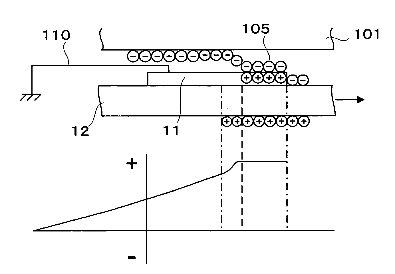
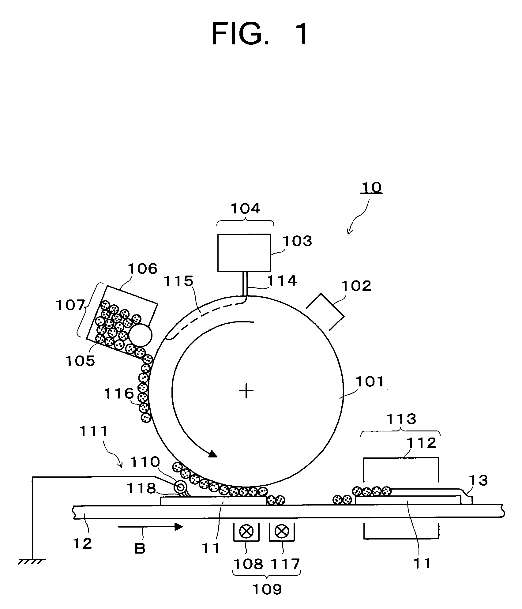
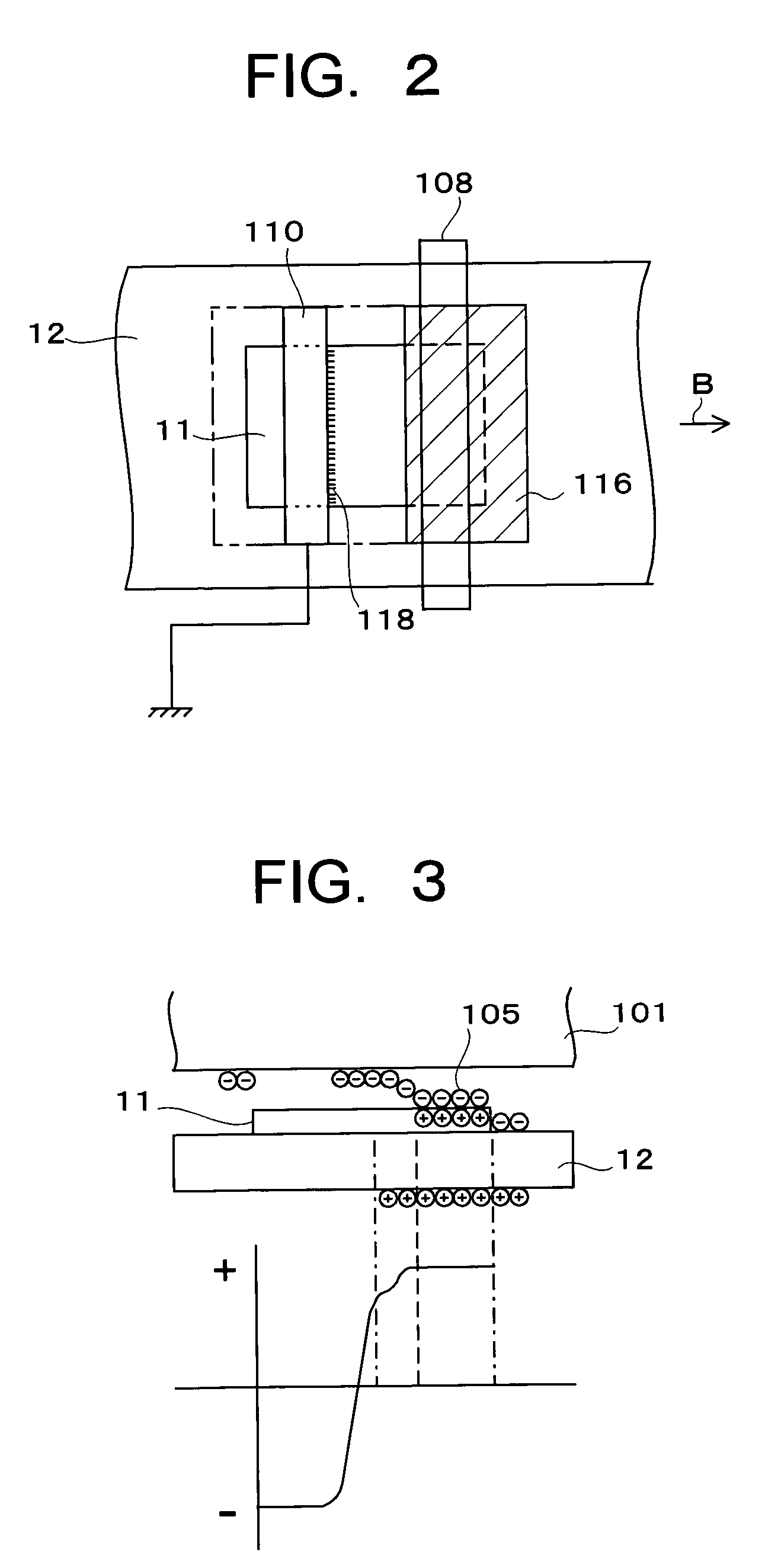
[0048]FIG. 1 and FIG. 2 are views showing the structure of an image forming apparatus according to the present invention. FIG. 1 is a front view schematically showing the structure of the image forming apparatus, and FIG. 2 is a plan view showing the essential structure of the image forming apparatus. An image forming apparatus 10 shown in these drawings, to which an electrophotographic system is applied, is used as a manufacturing apparatus of an electronic circuit, for example. The manufacturing apparatus of the electronic circuit is used for manufacturing an electronic circuit which has, for example, an insulating layer or a semiconductor layer as a circuitry layer 13 formed on a substrate 12 having a conductor layer 11.

[0049] The image forming apparatus 10 is mainly constituted of a photoconductive drum 101 having a photoconductive function, an electrifier 102, an exposure unit 104 having a laser generation / scan device 103, a developing unit 107 which has a developing machine 10...

fourth embodiment

[0083] Next, the operation of forming the image of the pattern information on a substrate P by using the image forming apparatus 40 will be explained with reference to a flowchart shown in FIG. 13. The following operation is controlled by the CPU 410. First, the photoconductor 401 is rotated in the direction of a narrow A in the drawing (ST1). Then, the photoconductor 401 is charged negative by the charging device 402 uniformly (ST2). Subsequently, the photoconductor 401 is exposed by the aligner 403 (ST3), and an electrostatic latent image based on the pattern information is formed on its surface. By the developing device 404, the electrostatic latent image on the photoconductor 1 is reversely developed by negative-charged toner to be a toner image (ST4).

[0084] The toner forming the toner image is made of binder containing metal particles. Thermoplastic resin is generally used as normal toner for electrophotography. However, according to the toner for forming the electronic circui...

fifth embodiment

[0102] The image forming apparatus 50 has a CPU 520 for governing entire control, a ROM 521 for storing a control program, a RAM 522 for storing data, and an operation unit 527 for interfacing with users. The CPU 520 responds to various instructions inputted by the user via the operation unit 527 to control the respective units in the image forming apparatus 50 comprehensively. Further, the image forming apparatus 50 has a laser driver 523 for driving a semiconductor laser oscillator (not shown) of an aligner 503 according to image data supplied from the exterior, a polygon motor driver 524 for driving a polygon motor (not shown) of the aligner 503, a carrier driving unit 525 for driving a transfer material carrier unit 507 to control the carry of a substrate P, a charging device 502, and a process controlling unit 526 for controlling each process of charging, developing and transferring by using developing devices 504A, 504B and a transferring device 508, and so on.

[0103]FIG. 18 i...


PUM

PropertyMeasurementUnit
Electric potential / voltageaaaaaaaaaa
Timeaaaaaaaaaa

Abstract

An image forming apparatus comprises an exposure unit forming an electrostatic latent image on a photoconductor based on image information, a developing unit developing the electrostatic latent image by toner made of formation material of a circuitry layer, and an electrostatic transferring unit transferring a toner image on the photoconductor onto a substrate. The toner image is transferred so as to cover at least a part of a conductor layer formed on the substrate. At this time, excessive charges caused in the conductor layer accompanying the start of the transfer of the toner image are removed. Alternatively, charges of which polarity is reverse to that of the toner are added to the conductor layer. These allow the circuitry layer to be formed to have a desired pattern favorably and securely on the conductor layer.

Description

CROSS-REFERENCE TO THE INVENTION [0001] This application is based upon and claims the benefit of priority from the prior Japanese Patent Application No. 2004-114059 filed on Apr. 8, 2004, Japanese Patent Application No. 2004-115795 filed on Apr. 9, 2004, and Japanese Patent Application No. 2004-163408 filed on Jun. 1, 2004; the entire contents of which are incorporated herein by reference. BACKGROUND OF THE INVENTION [0002] 1. Field of the Invention [0003] The present invention relates to an image forming apparatus to which an electrophotographic system is applied, and a method of manufacturing an electronic circuit using the same. [0004] 2. Description of the Related Art [0005] Conventionally, etching and screen printing methods have been heavily used in forming an electronic circuit applied to a wiring board, semiconductor element and the like. When the etching method is used to form a conductor pattern, exposure masks are necessary for respective layers. In the screen printing me...

Claims


Application Information

Patent Timeline
IPC IPC(8): G03G15/16G03G15/20H05K1/09H05K3/10H05K3/20H05K3/24
CPCG03G2215/00523Y10T29/49126H05K3/1266H05K3/207H05K3/246H05K2201/0347H05K2201/09781H05K2203/0517H05K2203/105G03G15/6591Y10T29/49128Y10T29/4913Y10T29/49155Y10T29/49165H05K1/095H04M1/0245H04M1/0208H04M2250/12
Inventor AOKI, HIDEOYAMAGUCHI, NAOKOTAKUBO, CHIAKIYAMAUCHI, TOSHIAKIIMAMIYA, KOJIHASHIZUME, HIROSHI
Owner KK TOSHIBA
Why Eureka
Try Eureka