Semiconductor device

a technology of semiconductor devices and semiconductors, applied in the direction of printed circuits, printed circuit components, printed circuit stress/warp reduction, etc., can solve the problems of deteriorating reliability of semiconductor devices, difficult realization of finer wiring, and insecure electrical connection between conductor layer b>4/b> and wiring layer b>6/b>, so as to prevent cracks and improve reliability on a product basis.

Active Publication Date: 2005-10-20
SHINKO ELECTRIC IND CO LTD
View PDF16 Cites 89 Cited by
  • Summary
  • Abstract
  • Description
  • Claims
  • Application Information

AI Technical Summary

Benefits of technology

[0012] An object of the present invention is to provide a semiconductor device which can prevent cracks from occurring even where

Problems solved by technology

However, since conventional printed wiring boards have needed large areas for the formation of via holes, flexibility in design has been limited, and thus finer wiring has been difficult to realize.
However, in the case where cracks spread all over the connection interface (i.e. rupture occurs at the connection interface), there arises a disadvantage in that the electrical connection between the conductor layer 4 and the wiring layer 6 is not secured.
This results in a deterioration in the reliability of the semiconductor device as a final product.
Moreover, there has

Method used


Image

  • Semiconductor device
  • Semiconductor device
  • Semiconductor device

Examples


first embodiment

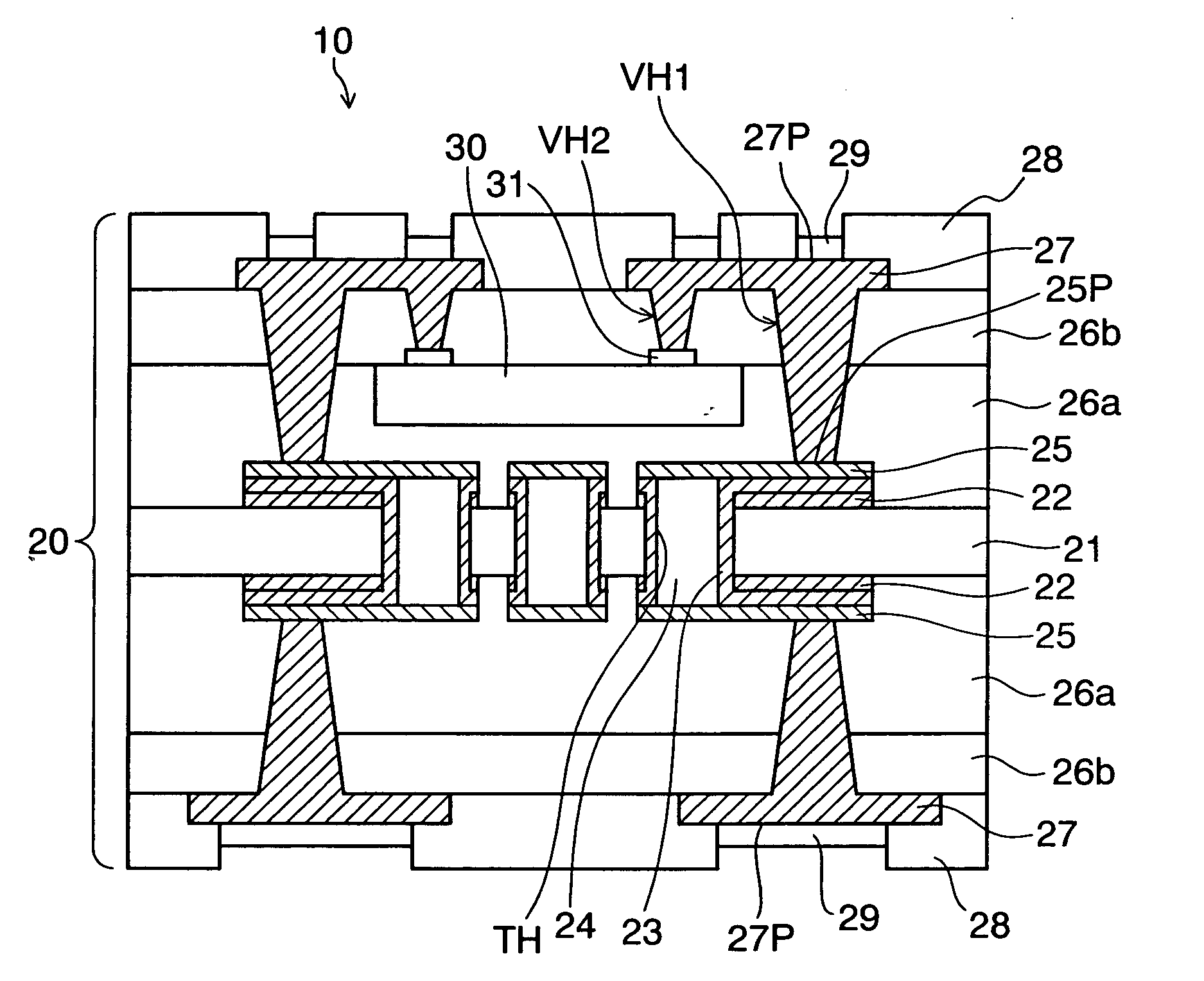
[0030]FIG. 1 schematically shows, in a cross-sectional view, the constitution of a semiconductor device according to the present invention.

[0031] The semiconductor device 10 according to this embodiment includes a wiring board 20 used as a package, and a semiconductor element (silicon (Si) chip) 30 mounted in the wiring board (package) 20 in an embedded manner. In the wiring board (package) 20, reference numeral 21 denotes an insulating base material (e.g., a glass cloth immersed in thermosetting resin, such as epoxy resin or polyimide resin) as a core substrate of this package; reference numeral 22 denotes a copper foil attached to each surface of the core substrate 21; reference numeral 23 denotes a plated layer of metal (e.g. copper (Cu)) formed on the copper foil 22 and the inner walls of through holes TH which are formed at specific positions in the core substrate 21 to pierce the core substrate 21 in the thickness direction; reference numeral 24 denotes an insulator (e.g. epox...

second embodiment

[0052]FIG. 6 schematically shows, in a cross-sectional view, the constitution of a semiconductor device according to the present invention.

[0053] As in the case of the first embodiment (FIG. 1), the semiconductor device 10a according to this embodiment includes a wiring board 20a used as a package, and the semiconductor chip 30 mounted in this wiring board (package) 20a in an embedded manner. Note, the semiconductor device (chip-embedded package) 10a according to this embodiment differs from the semiconductor device (chip-embedded package) 10 according to the first embodiment in that the wiring layer 27 is formed directly on the surface of the embedded chip 30 on which the electrodes 31 are formed.

[0054] Namely, in the first embodiment (FIG. 1), the electrodes 31 of the embedded chip 30 are connected to the wiring layer 27 through the via holes VH2 formed in the resin layer 26b; while, in this second embodiment (FIG. 6), the electrodes 31 of the embedded chip 30 are connected direc...

third embodiment

[0057]FIG. 9 schematically shows, in a cross-sectional view, the constitution of a semiconductor device according to the present invention.

[0058] As in the case of the first embodiment (FIG. 1), the semiconductor device 10b according to this embodiment includes a wiring board 20b used as a package, and semiconductor chips 30 and 40 mounted in this wiring board (package) 20b in an embedded manner. Note, the semiconductor device (chip-embedded package) 10b according to this embodiment differs from the semiconductor device (chip-embedded package) 10 according to the first embodiment in that the embedded chips 30 and 40 are placed at vertically symmetrical positions with respect to the core substrate 21.

[0059] Namely, in the first embodiment (FIG. 1), the chip 30 is merely embedded in the resin layer 26a; while, in this third embodiment (FIG. 9), the chips 30 and 40 are mounted in the resin layers 26a respectively in an embedded manner in the state where the chips 30 and 40 are glued w...


PUM


Abstract

In a semiconductor device, a plurality of wiring layers each patterned in a required shape are laminated over both surfaces of an insulating base material with insulating layers interposed therebetween, and electrically connected to one another through via holes piercing the insulating layers in the direction of thickness. A chip is mounted in an embedded manner in one insulating layer over at least one surface of the insulating base material. Electrodes of the chip are connected to one wiring layer. Through holes are formed in portions of the insulating base material, the portions corresponding to a mount area for the chip. Via holes are formed on outwardly extending portions (pad portions) of the wiring layer connected to a conductor layer formed at least on the inner walls of the through holes.

Description

CROSS-REFERENCE TO RELATED APPLICATIONS [0001] This application is based on and claims priority of Japanese Patent Application No. 2004-123998 filed on Apr. 20, 2004, the entire contents of which are incorporated herein by reference. BACKGROUND OF THE INVENTION [0002] (a) Field of the Invention [0003] The present invention relates to a semiconductor device. In particular, the present invention relates to a semiconductor device having a package structure in which a chip, such as a semiconductor element or electronic component, is mounted within a wiring board. In the following description, for convenience, a semiconductor device in which a chip is mounted within a wiring board is also referred to as a “chip-embedded package.”[0004] (b) Description of the Related Art [0005] In recent years, for printed wiring boards, weight reduction is required, and finer and denser wiring is required in order to mount a ball grid array (BGA), a pin grid array (PGA), a chip-sized package (CSP), or th...

Claims


Application Information

Patent Timeline
IPC IPC(8): H01L23/12H01L21/44H01L23/538H01L25/065H05K1/02H05K1/11H05K1/18H05K3/46
CPCH01L23/5389H01L24/24H01L2924/10253H01L2224/32225H01L2924/014H01L2924/01033H01L2924/01024H01L24/82H01L25/0657H01L2224/24051H01L2224/24226H01L2224/24227H01L2224/73267H01L2225/06524H01L2225/06541H01L2225/06572H01L2225/06582H01L2225/06596H01L2924/01029H01L2924/0103H01L2924/01078H01L2924/01079H05K1/0271H05K1/115H05K1/185H05K3/4602H05K2201/09536H05K2201/09609H05K2201/09781H01L2924/01005H01L2924/01006H01L2924/00H01L2224/04105H01L2924/12042H01L2924/351
Inventor SUNOHARA, MASAHIROUEDA, KEISUKE
Owner SHINKO ELECTRIC IND CO LTD
Why Eureka
Try Eureka