Flip chip package, semiconductor package with bumps and method for manufacturing semiconductor package with bumps

a chip and chip technology, applied in semiconductor devices, semiconductor/solid-state device details, electrical devices, etc., can solve the problems of not providing a package with a better thermal and electrical performance, and not dissipating heat, and achieve the effect of enhancing thermal and electrical performan

Inactive Publication Date: 2005-10-20
ADVANCED SEMICON ENG INC
View PDF7 Cites 27 Cited by
  • Summary
  • Abstract
  • Description
  • Claims
  • Application Information

AI Technical Summary

Benefits of technology

[0008] In view of the above-mentioned problems, this invention is to provide a flip chip package havi

Problems solved by technology

In addition, such packages can not dissipate the heat, arisen out of electronics systems with high power and high frequency devices formed therein,

Method used


Image

  • Flip chip package, semiconductor package with bumps and method for manufacturing semiconductor package with bumps
  • Flip chip package, semiconductor package with bumps and method for manufacturing semiconductor package with bumps
  • Flip chip package, semiconductor package with bumps and method for manufacturing semiconductor package with bumps

Examples


Embodiment Construction

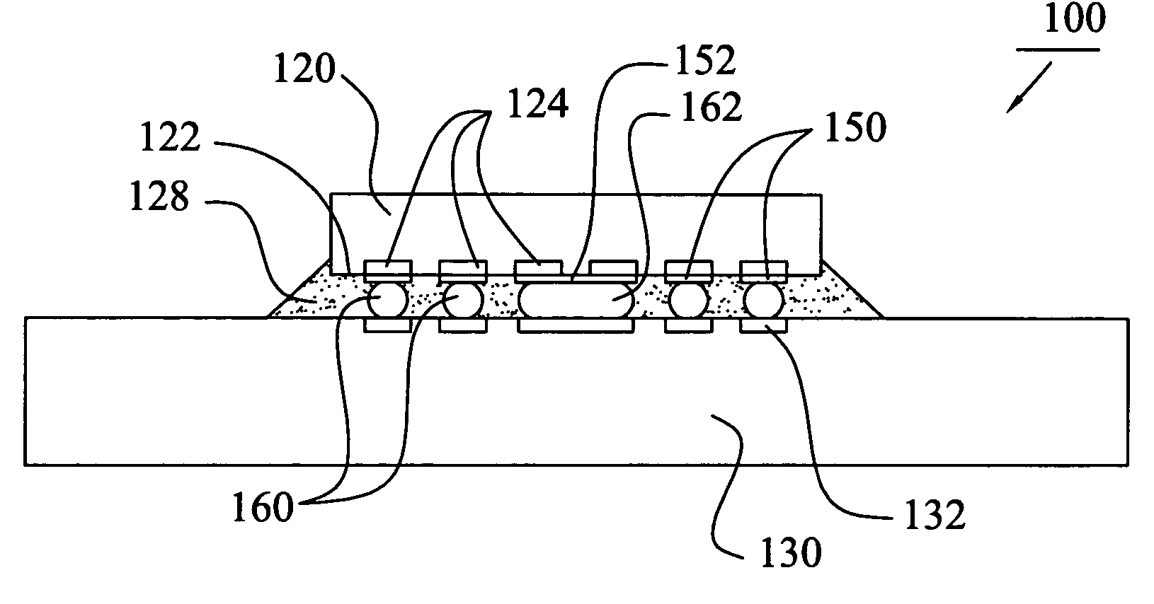
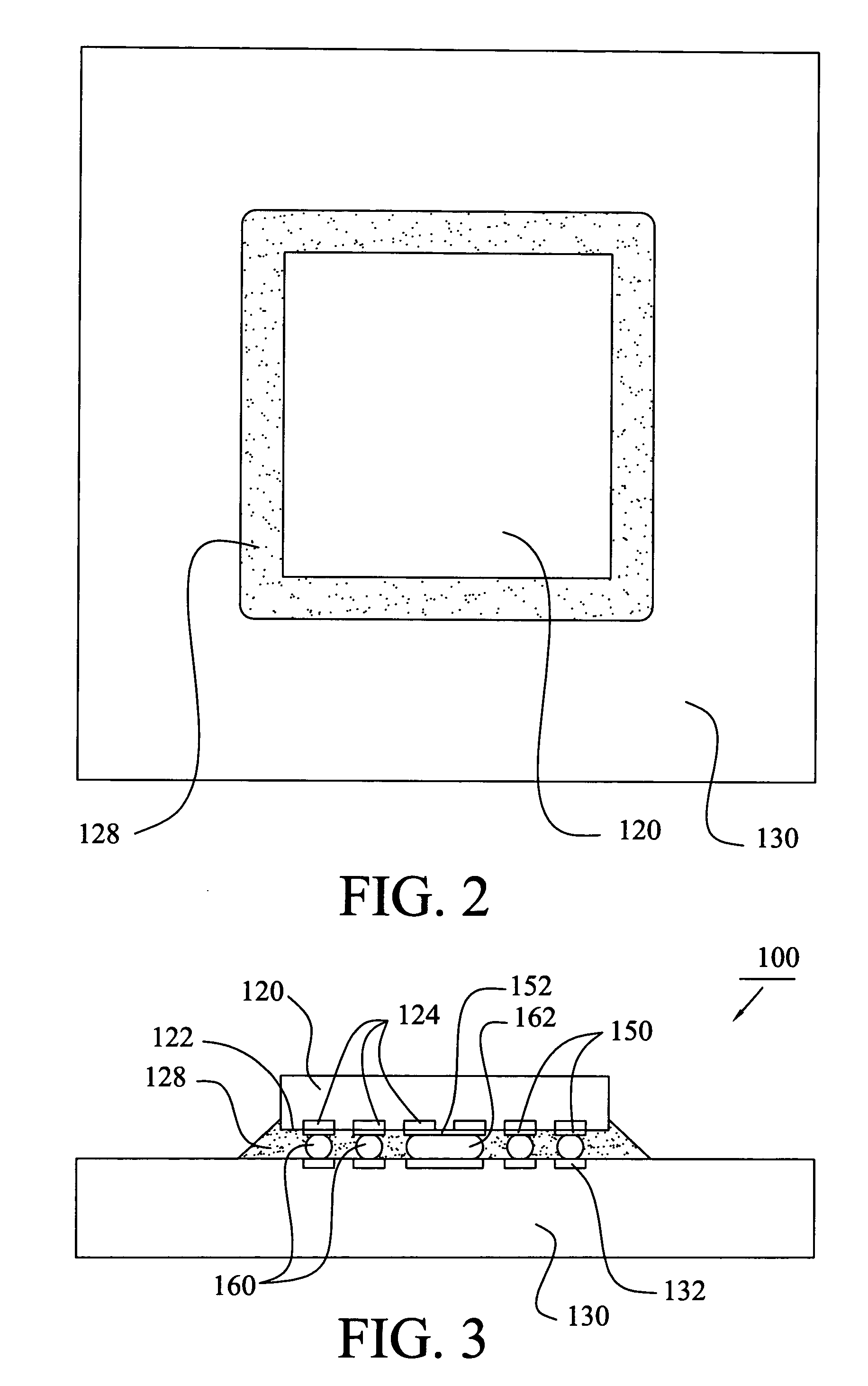
[0019] The flip chip package according to the preferred embodiments of this invention will be described herein below with reference to the accompanying drawings, wherein the same reference numbers are used in the drawings and the description to refer to the same or like parts.

[0020] As shown in FIGS. 2, 3 and 4, which illustrate a preferred embodiment of this invention. The flip chip package 100 mainly comprises a chip 120 flip-chip bonded to a substrate 130. Said chip 120 has an active surface 122 and a plurality of bonding pads 124 formed on the active surface 122. A plurality of bumps, including the solder bump 160 and the solder bar 162 as shown in FIGS. 3 and 4, are disposed over the bonding pads 124. A plurality of under bump metallurgy layers 150 and 152 formed between the bumps and the chip 120. To be more clearly, the under bump metallurgy layer 150 is substantially shaped into a circle and connected to the solder bump 160. In addition, the under bump metallurgy layer 152 ...


PUM


Abstract

A semiconductor chip with bumps formed therein comprises an active surface, a plurality of bonding pads, a passivation layer, a plurality of first UBMs (under bump metallurgy), a second UBM, a plurality of first bumps, and a plurality of second bumps. The bonding pads are disposed on the active surface of the semiconductor chip. The passivation layer covers the active surface of the semiconductor chip with the pads exposed out of the passivation layer. The first UMBs are individually disposed on the bonding pads. The second UMB is disposed on at least two of the bonding pads. The first bumps are disposed on the first UMBs. The second bumps are disposed on the second UBM.

Description

BACKGROUND OF THE INVENTION [0001] 1. Field of Invention [0002] This invention relates to a flip chip package. More particularly, the present invention is related to a flip chip package with solder bars formed therein. [0003] 2. Related Art [0004] A well-known semiconductor package, such as a flip chip package is applicable to communication products, portable electronics products, and packages for high-frequency chips. Referring to FIG. 1, it discloses a conventional and well-know flip chip package 10, which mainly comprises a chip 20 attached to a substrate 30 in a flip-chip bonding type. The chip 20 has an active surface 22 and a plurality of bonding pads 24 formed thereon. Besides, a plurality of bumps 26 electrically and mechanically connected to the contacts 32 of the substrate 30. The bumps 26 are formed by conventional bumping process and C4 technology (Controlled Collapse Chip Connection). Furthermore, an underfill 28 is disposed between the chip 20 and the substrate 30 and ...

Claims


Application Information

Patent Timeline
IPC IPC(8): H01L21/44H01L21/48H01L21/56H01L23/48H01L23/485H01L23/498
CPCH01L21/563H01L2224/14051H01L23/49838H01L2224/13099H01L2224/73203H01L2924/01029H01L2924/01082H01L2924/01322H01L2924/30107H01L2924/01006H01L2924/01033H01L2924/014H01L24/03H01L24/05H01L24/11H01L24/13H01L24/14H01L23/49816H01L2224/0401
Inventor TAO, SUHUANG, MIN-LUNGTONG, HO-MING
Owner ADVANCED SEMICON ENG INC
Why Eureka
Try Eureka