Semiconductor integrated circuit device and test method thereof

a technology of integrated circuit and integrated circuit device, which is applied in the direction of solid-state devices, instruments, and detecting faulty computer hardware, can solve the problems of increased circuit area and difficulty in automatic test pattern generation, and achieve the effect of accurate tes

Inactive Publication Date: 2005-10-20
NEC ELECTRONICS CORP
View PDF10 Cites 23 Cited by
  • Summary
  • Abstract
  • Description
  • Claims
  • Application Information

AI Technical Summary

Benefits of technology

[0056] According to the present invention, among the flip-flops in the logic circuit, flip-flops (indefinite state control flip-flops) for performing control for preventing propagation of an indefinite value to a test target path are selected. Then, the indefinite state control flip-flops are configured to form a chain different from those of normal scan flip-flops, and values for preven...

Problems solved by technology

However, in the case of the configuration in which the control circuits are added so as not to cause an indefinite value to influence the result of a test (refer to FIG...

Method used


Image

  • Semiconductor integrated circuit device and test method thereof
  • Semiconductor integrated circuit device and test method thereof
  • Semiconductor integrated circuit device and test method thereof

Examples


Embodiment Construction

[0067] In order to describe the present invention described above, embodiment of the present invention will be described below with reference to the appended drawings.

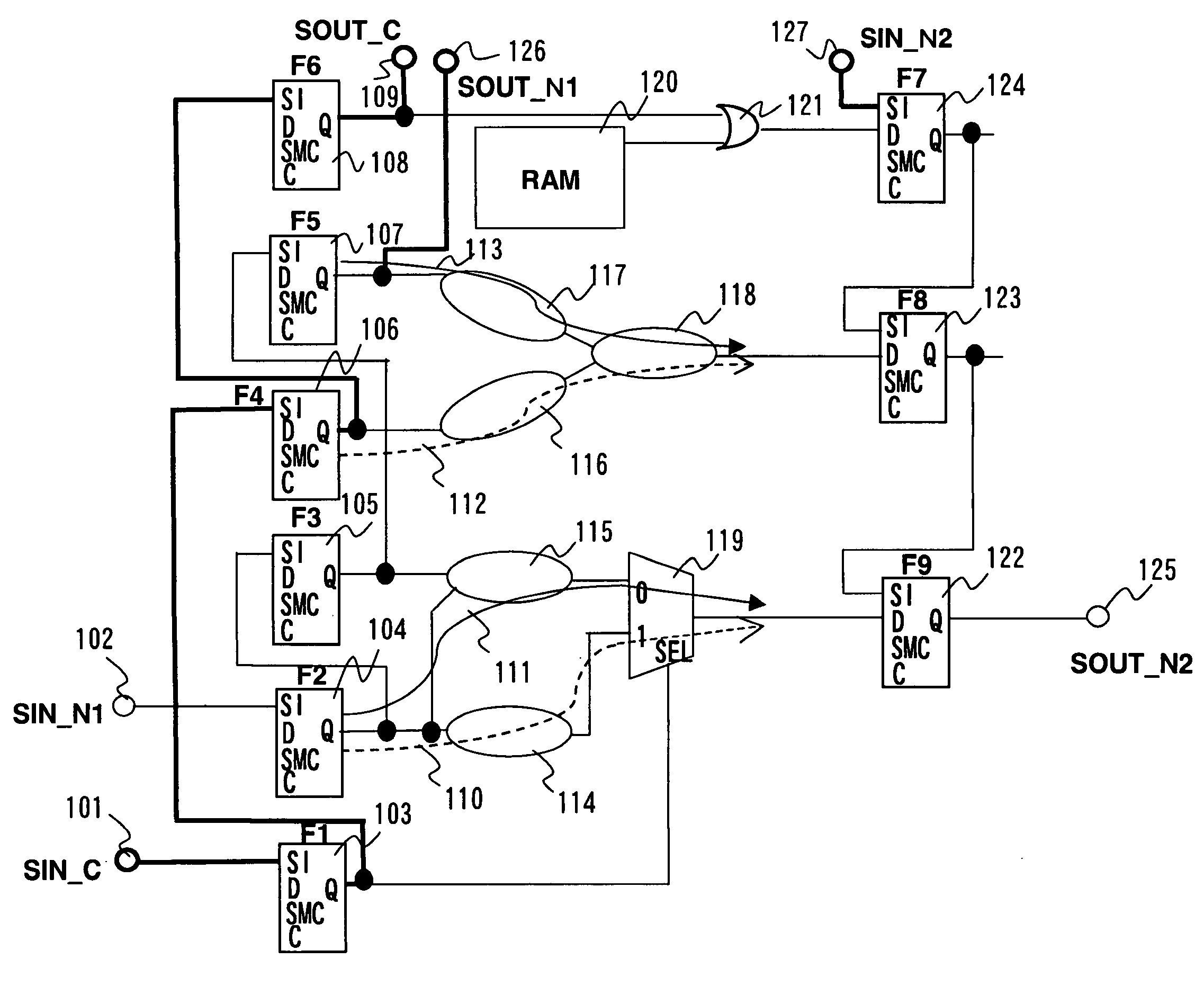
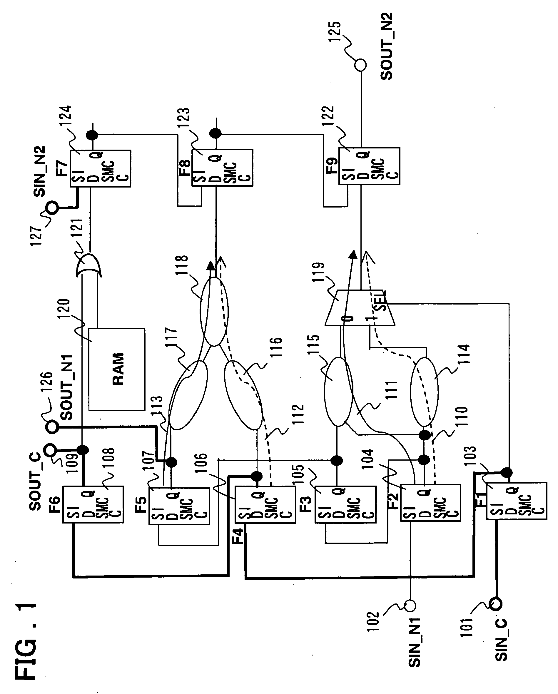
[0068]FIG. 1 is a diagram for explaining a configuration of an embodiment of the present invention. Referring to FIG. 1, flip-flops 104, 105, and 107 are serially connected when a scan mode control signal (SMC) indicates a scan mode. A path obtained by the serial connection constitutes a scan chain on an input side. Except for the time of the scan mode, each of the flip-flops 104, 105 and 107 performs a parallel operation in which a data signal at a data input terminal (D) thereof is sampled responsive to a clock signal from a clock input terminal (C) thereof for output from a data output terminal (Q) thereof.

[0069] Flip-flops 122, 123, and 124 are serially connected when the scan mode control signal (SMC) indicates the scan mode, and a path obtained by the serial connection constitutes a scan chain on an output side...


PUM


Abstract

Disclosed is a semiconductor integrated circuit device using a scan path test in which propagation of an indefinite value to a test target path is inhibited while suppressing an increase in a circuit area, and a test method thereof. When a plurality of flip-flops within a logic circuit is serially connected to form scan chains and a scan path test is conducted, one or a plurality of flip-flops within the logic circuit are provided as indefinite state control flip-flops for holding values for preventing an indefinite value from propagating through a test target path and being captured by the scan chain on an output side during the test. The indefinite state control flip-flops are serially connected based on a control signal, and constitute a chain of flip-flops, different from the scan chain of other flip-flops. A value serially input from an input terminal is set in the plurality of indefinite state control flip-flops, respectively.

Description

FIELD OF THE INVENTION [0001] The present invention relates to a semiconductor integrated circuit device and a test method thereof. More specifically, the invention relates to a scan path circuit and the test method thereof. BACKGROUND OF THE INVENTION [0002] As an approach to design for testability of a semiconductor integrated circuit, a scan path test is employed. In this test, a plurality of flip-flops provided in a logic circuit are serially connected to operate as a shift register, thereby conducting the test. As is well known, a flip-flop that constitutes a scan path (also referred to as a “scan flip-flop”) includes a serial input terminal (SI), a data input terminal (D), a data output terminal (Q), a clock input terminal (C), and a scan mode control terminal (SMC). When a signal input to the scan mode control terminal (SMC) indicates a scan mode (also referred to as a “serial mode”), the flip-flop samples an input signal at the serial input terminal (SI) thereof responsive t...

Claims


Application Information

Patent Timeline
IPC IPC(8): G01R31/28G01R31/317G01R31/3185G06F11/22H01L21/82H01L21/822H01L27/04
CPCG01R31/318536G01R31/31719
Inventor YAMAUCHI, HISASHI
Owner NEC ELECTRONICS CORP
Why Eureka
Try Eureka