

Method of manufacturing nano-wire
- Summary
- Abstract
- Description
- Claims
- Application Information
AI Technical Summary
Benefits of technology
Problems solved by technology
Method used
Image

Examples
Embodiment Construction
[0025] Now, the present invention will be described in more detail with reference to the attached drawings.
[0026] The present invention basically uses a seed having a steric structure.
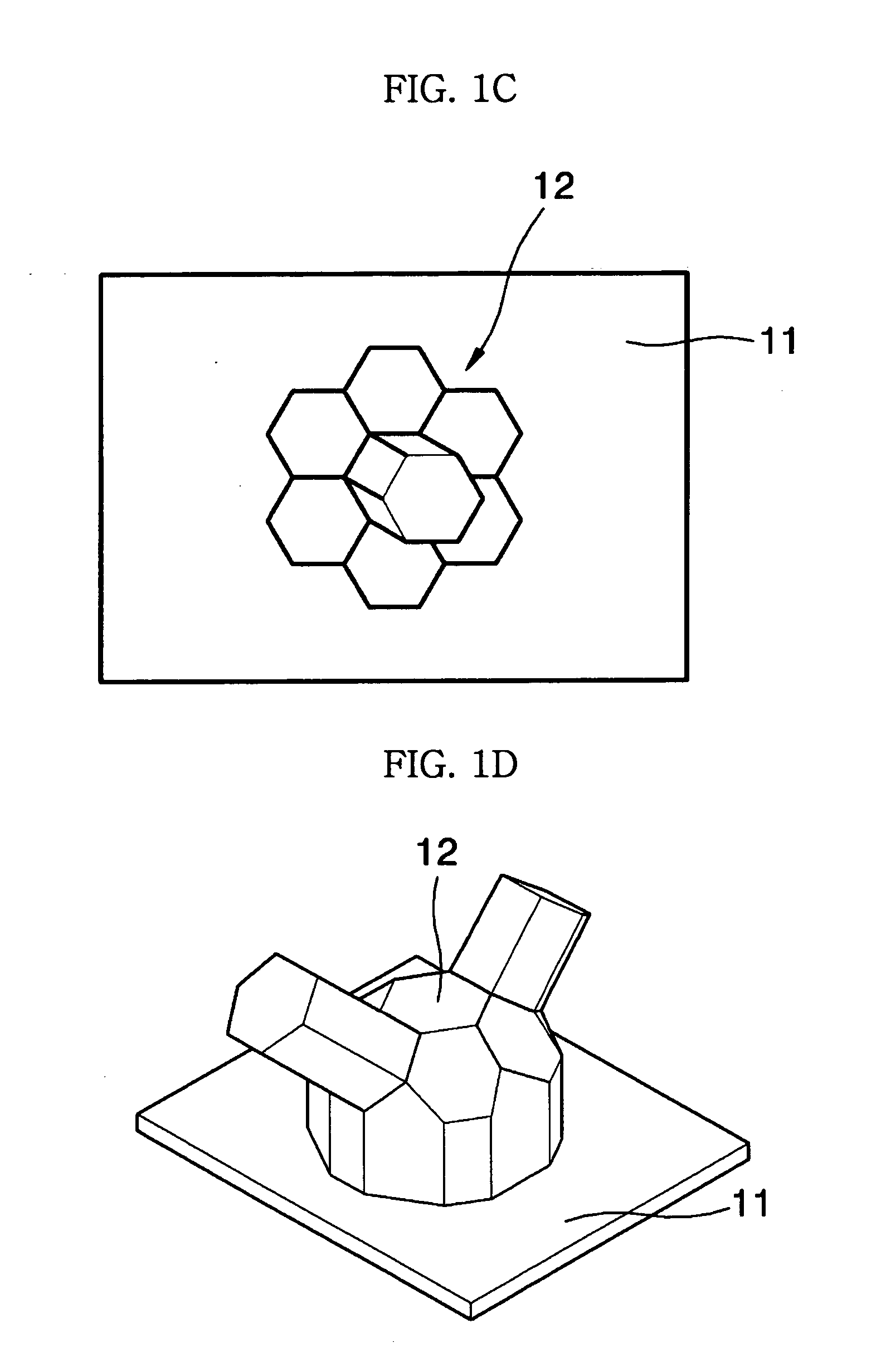
[0027] The seed having a steric structure has a predetermined crystal structure, and a wire to be grown is grown from a crystal face of the seed, and one or more wires can be grown from several crystal faces of the seed according to conditions.
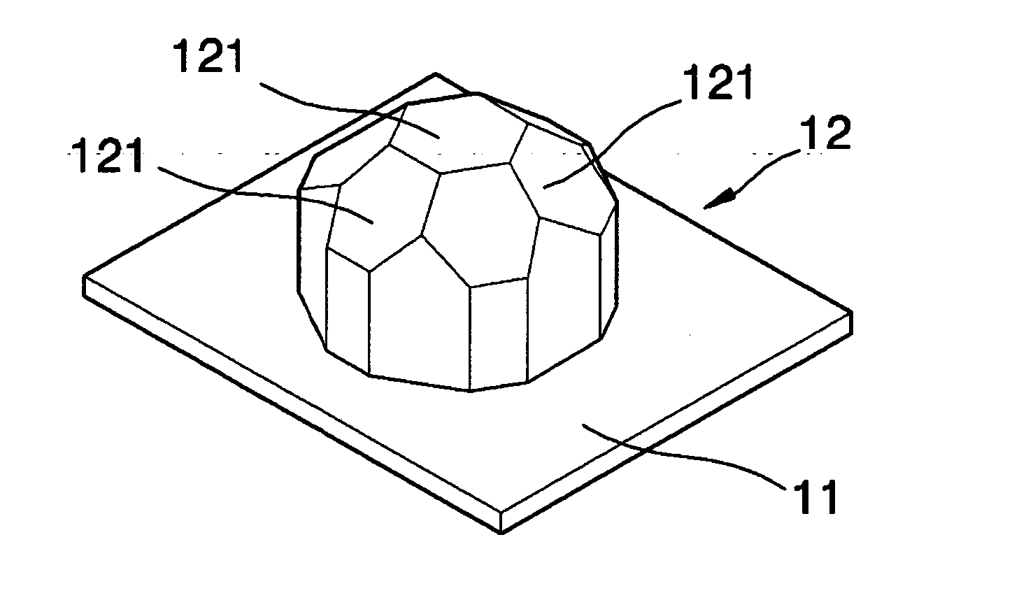
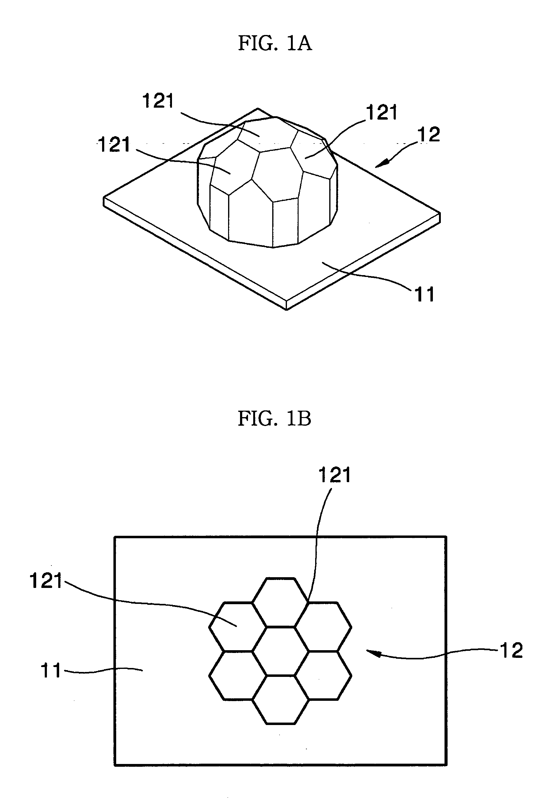
[0028] First, a crystal grain is prepared as a seed on a substrate. The crystal grain has a plurality of crystal faces and is directly grown from the substrate or is attached as a crushed crystal grain.
[0029] The crystal grain directly grown from the substrate is grown into an island shape on the substrate, for example, a silicon substrate by a chemical vapor deposition method, etc. A known method can be applied in growing a crystal of an island shape. Preferably, the chemical vapor deposition method among the known method can be applied in growing the crysta...
PUM
 Abstract
Description
Claims
Application Information