Organic electroluminescent device, method of manufacture thereof and electronic apparatus

Inactive Publication Date: 2005-10-27
SEIKO EPSON CORP
View PDF7 Cites 17 Cited by
  • Summary
  • Abstract
  • Description
  • Claims
  • Application Information

AI Technical Summary

Benefits of technology

[0029] By employing the configuration composed of the first film formed with the vapor deposition method and the second film formed thereon into a strip, the striped electrode can acquire a reliably increased thickness.
[0030] Furthermore, by forming an electrode with a droplet ejecting method, the accuracy in placing an electrode material is enhanced, and the film thickness of the electrode is inexpensively and easily increased.
[0031] In the above-described organic EL device, the above-described second film is formed so as not to contact with both of two adjacent separators among the separators, so that the short circuit between electrodes through the separator is reliably prevented.
[0032] In addition, the above-described second film is formed so as to contact with

Problems solved by technology

A display device having a striped electrode structure tends to cause a voltage drop in an ex

Method used


Image

  • Organic electroluminescent device, method of manufacture thereof and electronic apparatus
  • Organic electroluminescent device, method of manufacture thereof and electronic apparatus
  • Organic electroluminescent device, method of manufacture thereof and electronic apparatus

Examples


first embodiment

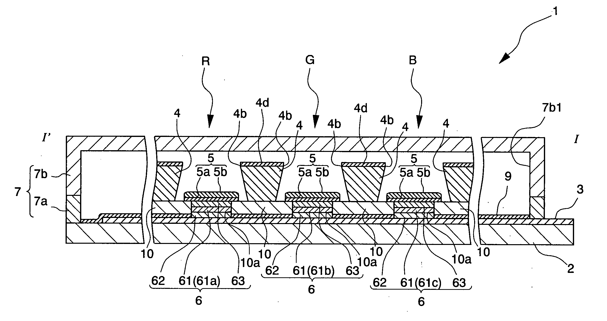
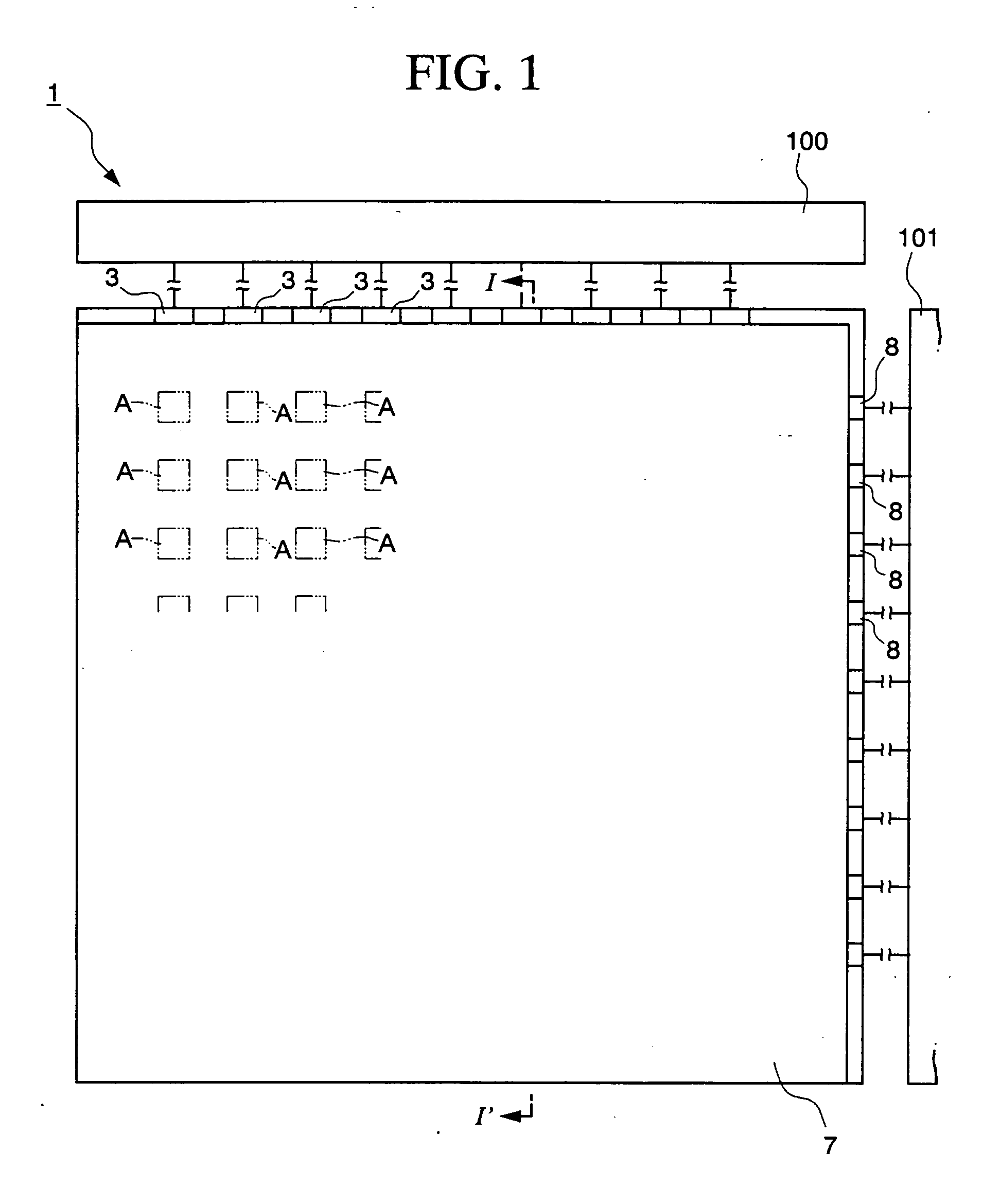
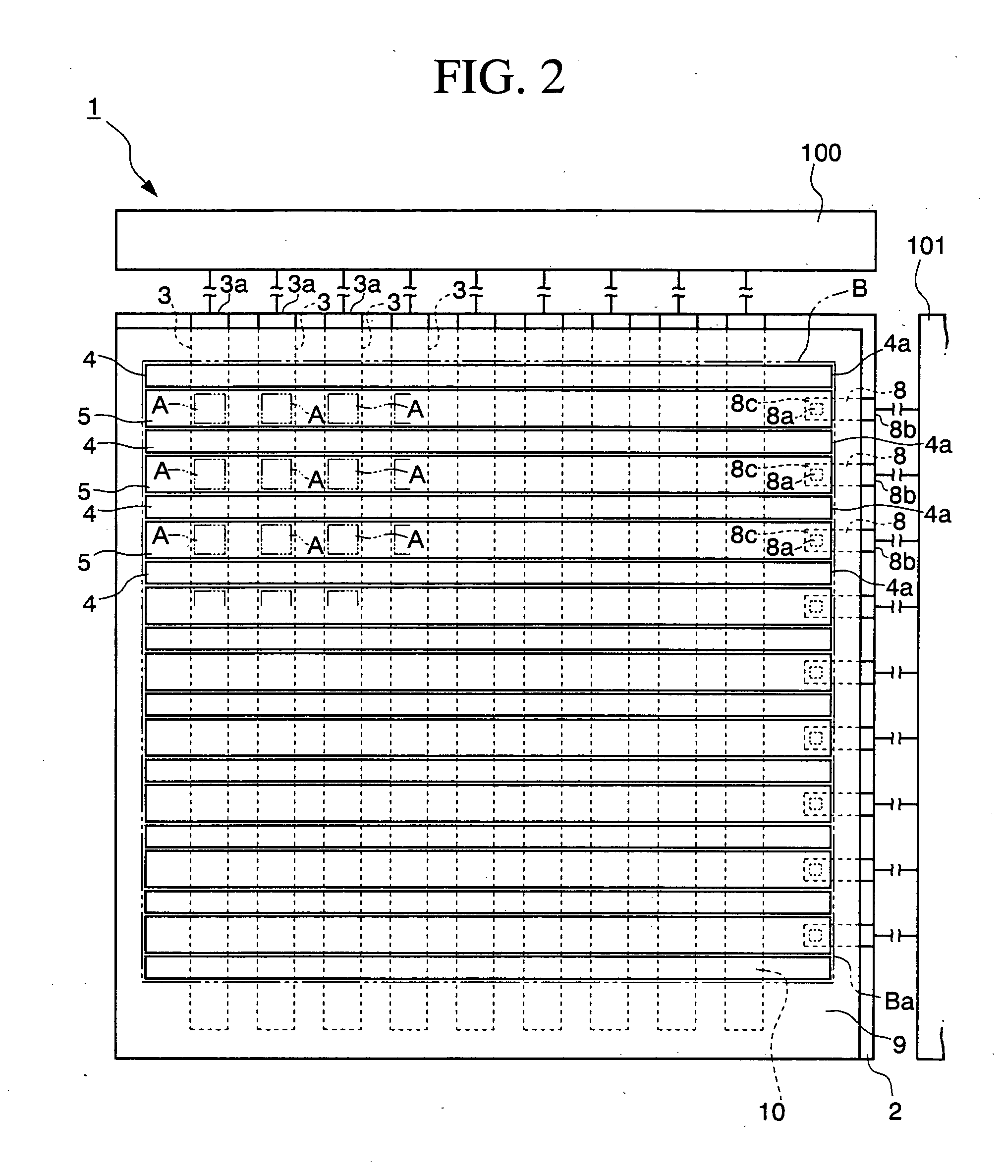
[0055] FIGS. 1 to 3 are schematic block diagrams which schematically show a passive matrix type organic EL (electroluminescent) display device according to the present embodiment. FIG. 1 is a plan view, FIG. 2 is an inner block diagram of an organic EL device 1, and FIG. 3 is a view on an arrow of I-I′ in FIG. 1. As shown in these drawings, the present organic EL device 1 mainly includes: a plurality of first electrodes (anodes) 3 with a strip extending to a predetermined direction on a substrate 2; a plurality of cathode separators (separators) 4 extending to the direction perpendicular to the extending direction of the first electrodes; a bank layer 10 arranged below the cathode separators 4; second electrodes (cathodes) 5 formed between the cathode separators 4; an organic functional layer 6 sandwiched between the first electrode 3 and the second electrode 5 from the top and the bottom, in a crossing area A (a light-emitting area) of the first electrode 3 and the second electrode...

second embodiment

[0099] In the following, the second embodiment of an organic EL device according to the present invention will be described with reference to FIG. 15.

[0100] In the present embodiment, as shown in FIG. 15, the second electrode 5 has the layered structure consisting of the first film 5a, the second film 5b and the third film 5c. A step for manufacturing the organic EL device 1 includes, in the step for forming the second electrode 5, repeating (twice in the present embodiment) the steps of placing an electrode material with a droplet ejecting method, on the electrode film (the first film 5a) formed by a vapor deposition method, and the step of drying the placed electrode material. Specifically, the step includes forming the second film 5b with the droplet ejecting method on the first film 5a formed by the vapor deposition method, and further forming the third film 5c on the second film 5b with the droplet ejecting method. In thus composed organic EL device 1, the second electrode 5 h...

third embodiment

[0101] In the following, the third embodiment of an organic EL device according to the present invention will be described with reference to FIGS. 16 to 18.

[0102] In the present embodiment, as shown in FIG. 16, the second electrode 5 has a layered structure composed of the first film 5a and the second film 5b. The first film 5a is formed by a vapor deposition method, and the second film 5b is formed by a droplet ejecting method. In addition, the second film 5b is formed so as to contact with one of two adjacent cathode separators 4 among a plurality of cathode separators 4, and not to contact with the other. Thereby, in the present embodiment as well, even though an electrode film (an evaporated film) is formed on the top surface 4d of the cathode separator 4, the short circuit between the second electrodes 5 through the cathode separator 4 is prevented.

[0103] A step for manufacturing the organic EL device 1 includes, in the step for forming the second electrode 5, as shown in FIG...


PUM


Abstract

A method for manufacturing an organic electroluminescent device having an organic functional layer formed between facing electrodes, the method includes forming separators which separate either of the electrodes into a strip, forming an electrode film between the separators with a vapor deposition method, and placing a further electrode material on the electrode film which is formed between the separators with the vapor deposition method.

Description

BACKGROUND OF THE INVENTION [0001] 1. Field of the Invention [0002] The present invention relates to an organic electroluminescent device, a method of manufacture thereof and an electronic apparatus. [0003] Priority is claimed on Japanese Patent Application No. 2004-125402, filed Apr. 21, 2004, the content of which is incorporated herein by reference. [0004] 2. Description of Related Art [0005] In recent years, in electronic apparatuss such as notebook computers, mobile phones and electronic notes, a display device provided with an organic electroluminescent (hereafter called organic EL) element in correspondence with a picture element, such as an organic EL device, has been proposed as device for displaying information. [0006] One of such organic EL devices is a passive matrix type (a simple matrix type) organic EL device. Generally, the passive matrix type organic EL device includes a plurality of first electrodes formed into a strip extending in a predetermined direction on a sub...

Claims


Application Information

Patent Timeline
IPC IPC(8): H01J1/62H01J63/04H05B33/10H01L27/32H01L51/00H01L51/50H01L51/52H05B33/12H05B33/14H05B33/22H05B33/26
CPCH01L27/3281H01L51/5221H01L51/0021H01L27/3295H10K59/17H10K59/173H10K59/122H10K71/60H10K50/82E04F13/005E04C2/284E04C2/38
Inventor SAKAI, HIROFUMISAKURAI, KAZUNORI
Owner SEIKO EPSON CORP
Why Eureka
Try Eureka