Semiconductor device characteristics measurement apparatus and connection apparatus

a technology of electromagnetic field and measurement apparatus, which is applied in the direction of measurement devices, electronic circuit testing, instruments, etc., can solve the problems of difficult to accurately measure the electrical characteristics of dut b>50, inefficient measurement operation, etc., and achieve accurate measurement of a minute current range, increase measurement accuracy, and enhance measurement convenience

Active Publication Date: 2005-10-27
KEYSIGHT TECH
View PDF3 Cites 19 Cited by
  • Summary
  • Abstract
  • Description
  • Claims
  • Application Information

AI Technical Summary

Benefits of technology

[0028] According to the present invention, it is possible to configure a measurement system that offers enhanced convenience in measurement and that provides increased measurement accuracy compared to the known examples described above. In addition, since the micro-current detecting means is located in the vicinity of the DUT, it is possible to accurately measure a minute current range as small as femto-amperes or less.
[0029] When the connection ap

Problems solved by technology

However, the example also suffers from the drawback that measurement operation is inefficient, since the operator needs to manually replace the c

Method used


Image

  • Semiconductor device characteristics measurement apparatus and connection apparatus
  • Semiconductor device characteristics measurement apparatus and connection apparatus
  • Semiconductor device characteristics measurement apparatus and connection apparatus

Examples


Embodiment Construction

[0042] Preferred embodiments according to the present invention will be described below with reference to the accompanying drawings.

[Basic Configuration]

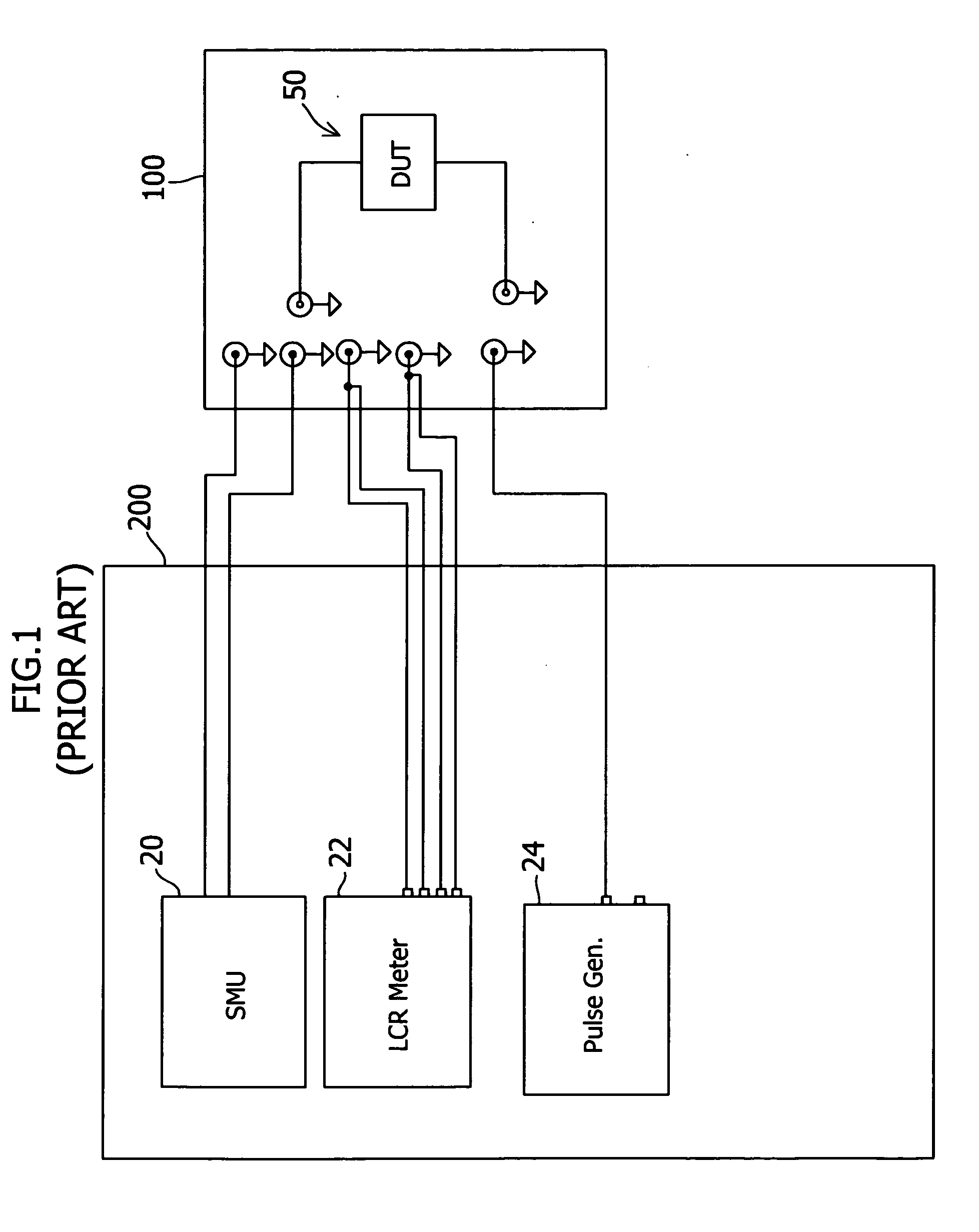
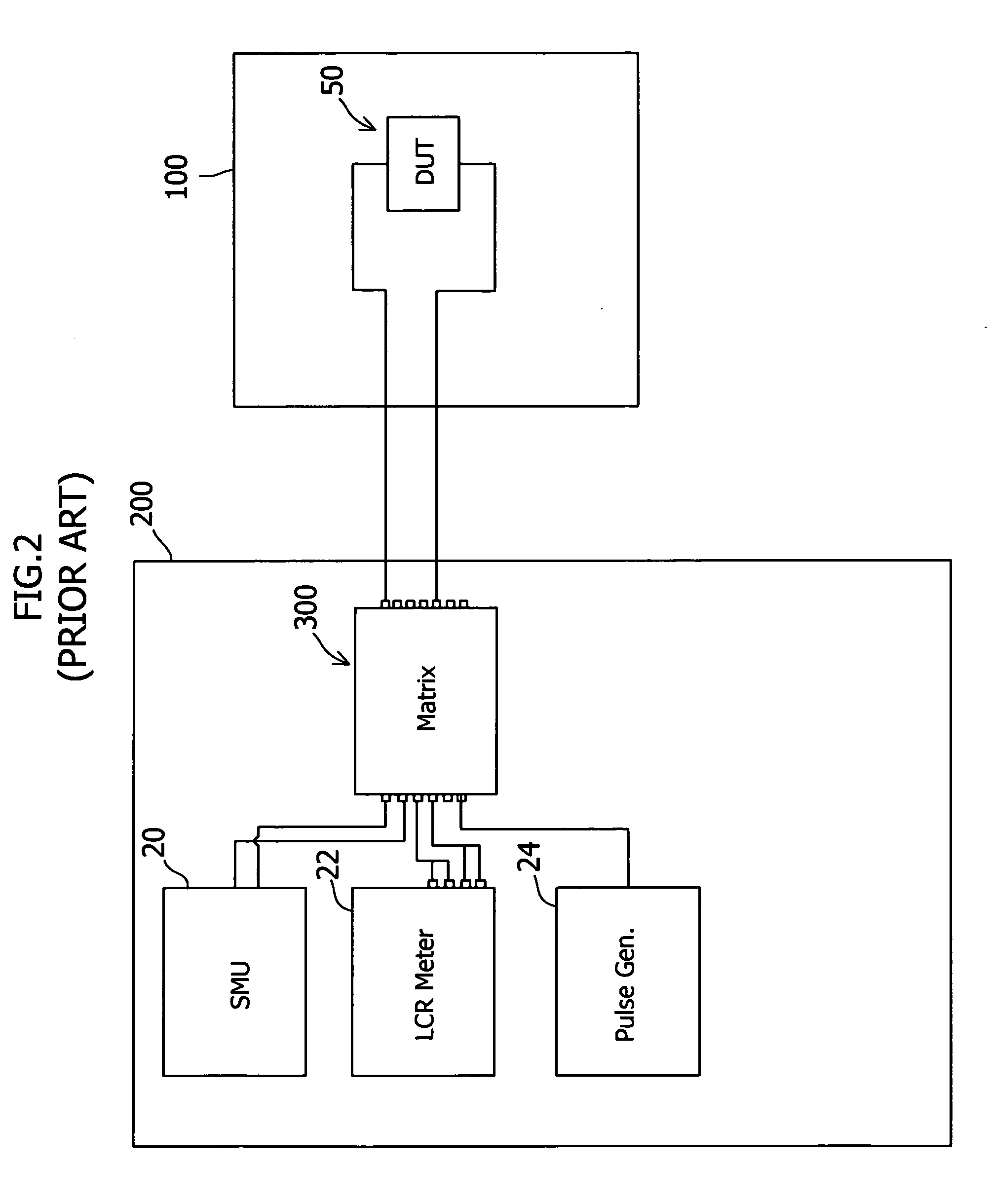
[0043]FIG. 3 is a block diagram showing the configuration of an embodiment for measuring capacitance in the present invention. FIG. 3 shows a block configuration in which an SMU (source monitor units or source measure unit) 20, an LCR (inductance-capacitance-resistance) meter 22, and a pulse generator 24, which are mounted in an equipment rack 200, are used to measure electrical characteristics of a DUT (device under test) 50. The DUT 50 is mounted on a probe apparatus 100 so as to be probed. For convenience, the terms “positive (+) side” and “negative (−) side” are used for terminals of the DUT 50 and apparatuses to distinguish between its connections therewith. These expressions, however, are not particularly intended to mean a high potential and a low potential.

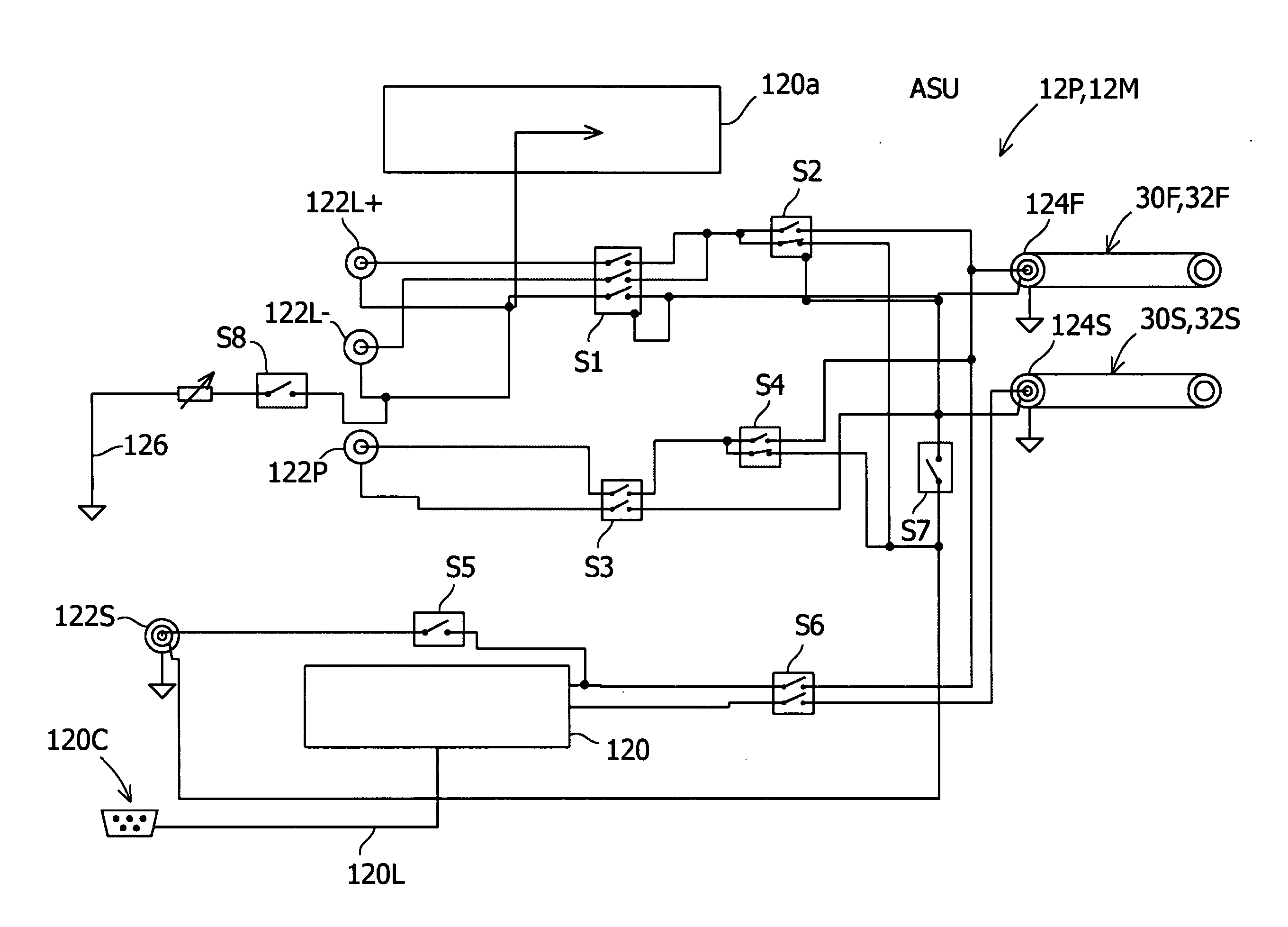
[0044] A switching portion 12 has an atto (attoampere) sense unit ...


PUM


Abstract

A semiconductor-device characteristic measurement apparatus includes first measuring means for measuring a first electrical characteristic of a device under test, second measuring means, switching means for switching between the first measuring means and the second measuring means such that one of the measuring means is connected to the device under test, and controlling means for controlling the switching means. The switching means includes switches that switch between a first wiring configuration for electrically connecting the first measuring means to the device under test and a second wiring configuration for electrically connecting the second measuring means to the device under test. The switching means is electrically connected to the device under test at a position closer to the device under test than the first measuring means and the second measuring means.

Description

BACKGROUND OF THE INVENTION [0001] 1. Field of the Invention [0002] The present invention relates to a measurement apparatus for an electronic device. More specifically, the present invention relates to a measurement apparatus for semiconductor device characteristics of an integrated circuit device or discrete electronic circuit device, and to a connection apparatus used for such measurement. [0003] 2. Description of the Related Art [0004] Conventionally, the related technologies shown in FIGS. 1 and 2 have been known as apparatuses for measuring the electrical characteristics of a device to be tested (or “device under test”, hereinafter referred to as DUT), such as integrated circuit devices and discrete electronic circuit devices consisting of semiconductors. [0005]FIG. 1 shows a known example of an apparatus for measuring electrical characteristics by causing a probe apparatus 100 to probe a DUT 50. In this known example, a current-voltage characteristic measurement unit 20 (or a...

Claims


Application Information

Patent Timeline
IPC IPC(8): G01R31/26G01R31/28
CPCG01R31/2844
Inventor TANIDA, SHINICHISHIMIZU, HIROYUKI
Owner KEYSIGHT TECH
Why Eureka
Try Eureka