Growth of high-k dielectrics by atomic layer deposition

a technology of atomic layer deposition and dielectric film, which is applied in the direction of chemical vapor deposition coating, coating, coating process, etc., can solve the problem that prior art fabrication techniques such as chemical vapor deposition (cvd) are increasingly incapable of meeting the requirements of forming these advanced thin films, and the tunneling leakage current becomes significant. , to achieve the effect of suppressing interfacial oxide growth and reducing the concentration of ozon

Inactive Publication Date: 2005-10-27
SENZAKI YOSHIHIDE +2
View PDF3 Cites 50 Cited by
  • Summary
  • Abstract
  • Description
  • Claims
  • Application Information

AI Technical Summary

Benefits of technology

[0010] In general, the present invention provides a method of depositing high-k dielectric films or layers, such as but not limited to high-k gate dielectric films. In one embodiment, atomic layer deposition (ALD) cycles are carried out where ozone is selectively conveyed to a chamber in separate cycles to form a metal oxide layer on the surface of a substrate where the metal oxide layer has an interfacial oxide layer of minimal thickness.
[0011] In one aspect of the present invention, a method of depositing a gate dielectric on a substrate using atomic layer deposition is provided carried out by the steps of: independently pulsing one or more chemical precursors, such as metal containing precursors, and ozone to a chamber, said ozone being pulsed at a high concentration and then reducing the concentration of ozone after one or more oxide layers have been formed on the substrate.
[0012] In another aspect of the present invention, one or more substrates are placed in an ALD react

Problems solved by technology

As oxide films are scaled down, the tunneling leakage current becomes significant and limits the useful range for SiO2 gate oxides to about 1.8 nm or more.
However, prior art fabrication techniques such as chemical vapor deposition (CVD) are increasingly unable to meet the requirements of forming these advanced thin films.
While CVD processes can be tailored to provide conformal films with improved step coverage, CVD processes often require high processing temperatures, result in incorporation of high impurity concentrations, and have poor precursor or reactant utilization efficiency.
For instance, one of the obstacles in fabricating high-k gate dielectrics is the formation of an interfacial silicon oxide layer during CVD processing.
Interfacial oxide growth problems for gate and capacitor diel

Method used


Image

  • Growth of high-k dielectrics by atomic layer deposition
  • Growth of high-k dielectrics by atomic layer deposition
  • Growth of high-k dielectrics by atomic layer deposition

Examples


Embodiment Construction

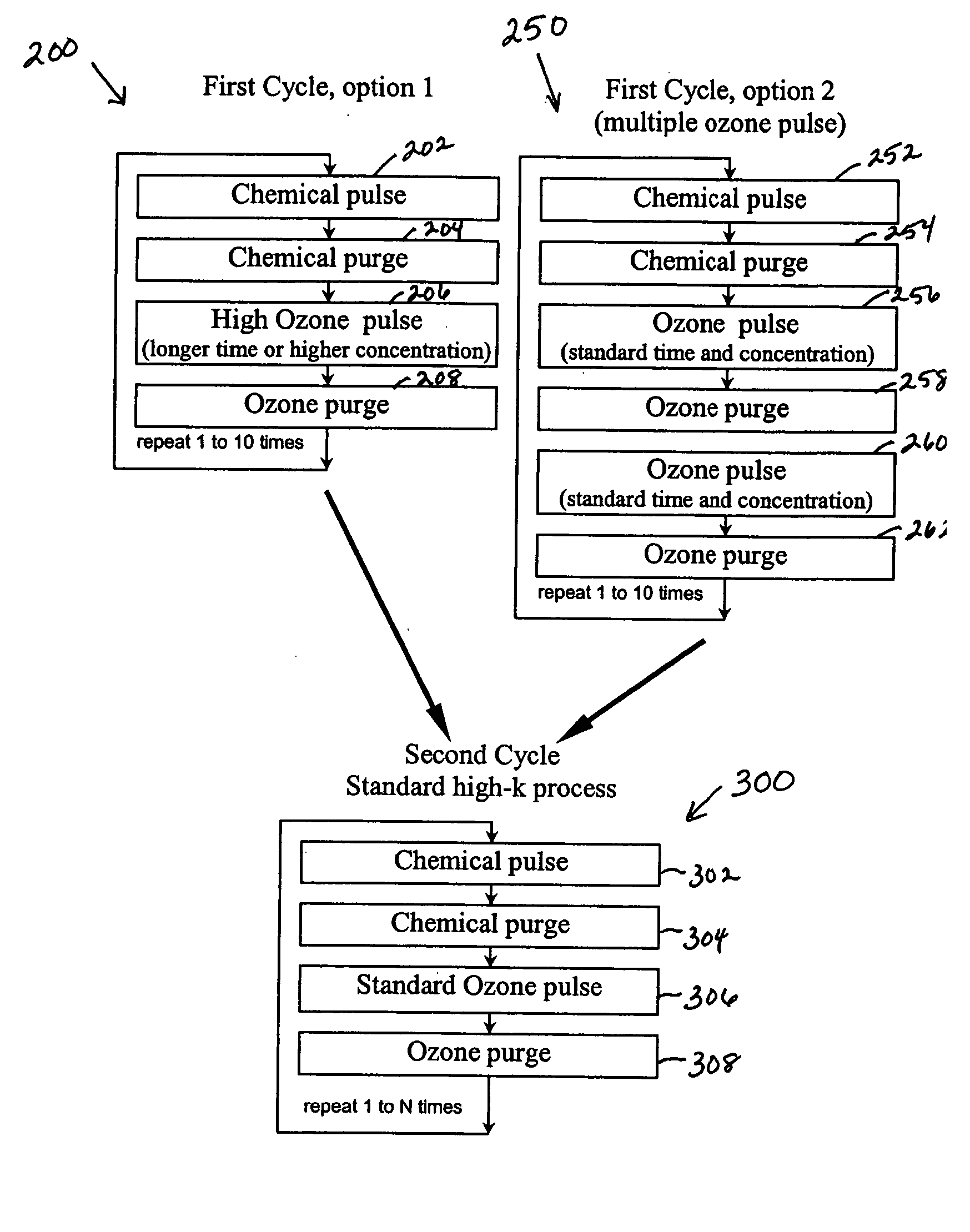
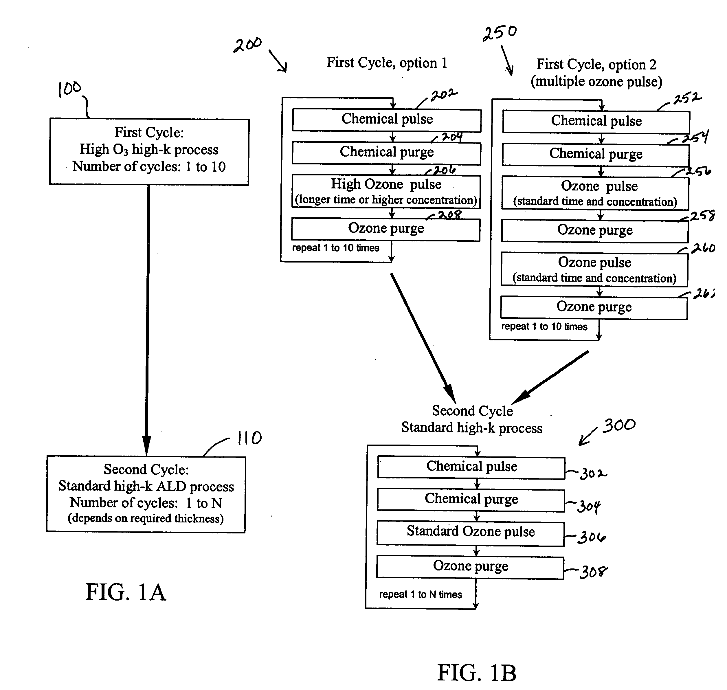
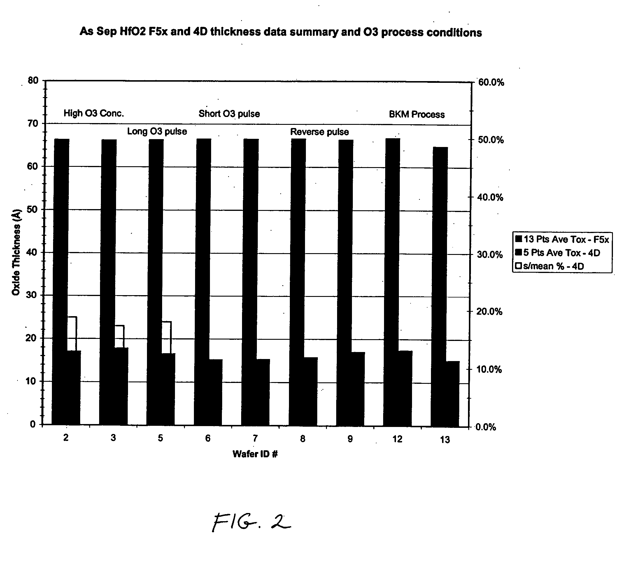
[0021] In general, the present invention provides atomic layer deposition (ALD) cycles carried out where ozone is selectively conveyed to a chamber in separate cycles to form substantially continuous oxide layer on the surface of a substrate where the oxide layer has an interfacial oxide layer of minimal thickness. In one embodiment, the interfacial oxide layer has a thickness of one monolayer. Preferably the interfacial oxide layer does not exceed a monolayer.

[0022] In one aspect of the present invention, a method of depositing a gate dielectric on a substrate using atomic layer deposition is provided by the steps of: independently pulsing one or more chemical precursors and ozone to a chamber, said ozone being pulsed at a high concentration and then reducing the concentration of ozone after one or more metal oxide layers have been formed on the substrate.

[0023] In another aspect of the present invention, one or more substrates are placed in an ALD reactor or chamber. In a first ...


PUM

PropertyMeasurementUnit
Temperatureaaaaaaaaaa

Abstract

In general, the present invention provides a method of depositing high-k dielectric films or layers, such as but not limited to high-k gate dielectric films. In one embodiment, atomic layer deposition (ALD) cycles are carried out where ozone is selectively conveyed to a chamber in separate cycles to form a metal oxide layer on the surface of a substrate where the metal oxide layer has an interfacial oxide layer of minimal thickness.

Description

CROSS REFERENCE TO RELATED APPLICATIONS [0001] This application claims the benefit of and priority to U.S. Provisional Patent application Ser. No. 60 / 507,875 filed on Sep. 30, 2003, entitled Two Step Sequential Growth of High-k Gate Dielectrics by Atomic Layer Deposition, the entire disclosure of which is hereby incorporated by reference. This application is related to Patent Cooperation Treaty Patent application no. PCT / JUS03 / 22712, entitled Atomic Layer Deposition of High k Dielectric Films, the entire disclosure of which is hereby incorporated by reference.FIELD OF THE INVENTION [0002] This invention relates generally to atomic layer deposition methods and systems. More specifically, the invention relates to a method of forming high dielectric constant (high-k) dielectric films or layers by atomic layer deposition. BACKGROUND OF THE INVENTION [0003] Semiconductor devices of future generation require thin dielectric films for metal oxide silicon (MOS) transistor gates, and capacit...

Claims


Application Information

Patent Timeline
IPC IPC(8): C23C16/40C23C16/455H01LH01L21/314H01L21/316H01L21/44
CPCC23C16/403C23C16/405C23C16/45527C23C16/45529C23C16/45531H01L21/31645H01L21/02181H01L21/0228H01L21/02337H01L21/3141H01L21/3162H01L21/02178
Inventor SENZAKI, YOSHIHIDELEE, SANG-INAL-LAMI, SATTAR
Owner SENZAKI YOSHIHIDE
Why Eureka
Try Eureka