Organic thin film transistor including organic acceptor film

a thin film transistor and organic technology, applied in transistors, solid-state devices, thermoelectric devices, etc., can solve the problems of lowering charge mobility, lattice distortion of the interior of crystals, and low charge mobility of organic tft, so as to improve the charge mobility of organic semiconductor films

Inactive Publication Date: 2005-11-03
SAMSUNG DISPLAY CO LTD
View PDF5 Cites 53 Cited by
  • Summary
  • Abstract
  • Description
  • Claims
  • Application Information

AI Technical Summary

Benefits of technology

[0018] The present invention provides an organic thin film transistor (T

Problems solved by technology

An organic TFT has the disadvantage of low charge mobility.
Once an organic semiconductor active film is oxidized, its coupling structure is broken, lowering charge mobility and causing lattice distortion of the interior of crystals.
As a result, charge traps are formed so as to provoke charge scattering, which further deteriorates charge mobility.
However, this me

Method used


Image

  • Organic thin film transistor including organic acceptor film
  • Organic thin film transistor including organic acceptor film
  • Organic thin film transistor including organic acceptor film

Examples


Embodiment Construction

[0042] Hereinafter, an organic thin film transistor (TFT) according to exemplary embodiments ofthe present invention will be described with reference to the attached drawings.

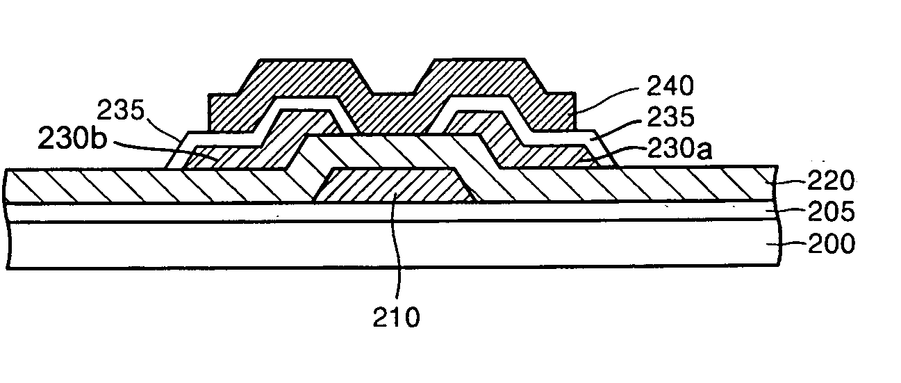
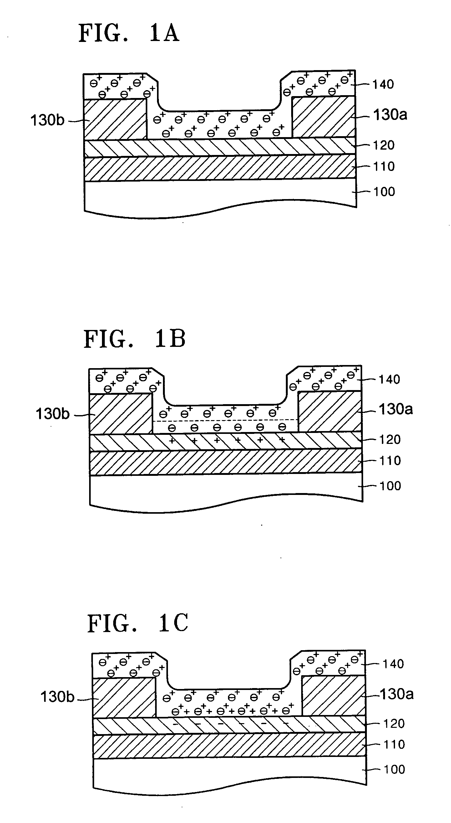
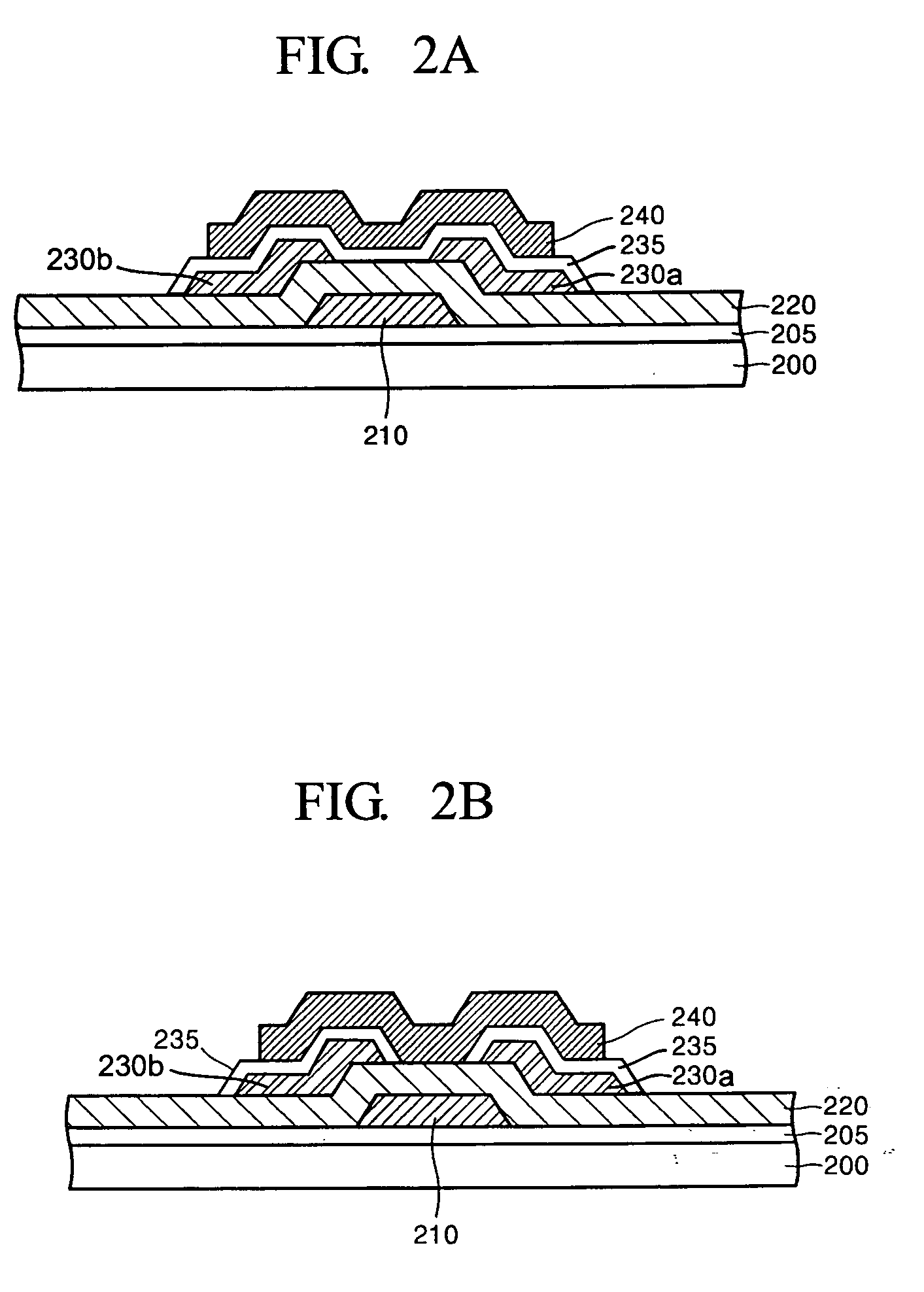
[0043]FIGS. 1A thru 1C are conceptual diagrams illustrating the principle on which an organic TFT operates. Generally, the organic TFT is structurally similar to a silicon transistor. Like a field effect transistor (FET), the organic TFT operates on the principle that, when a voltage is applied to a gate 110, an electric field is applied to a gate insulating film 120. A current flowing through the organic TFT is obtained by applying a voltage between a source region 130a and a drain region 130b. In this case, the source region 130a is grounded and supplies electrons or holes. The semiconductor active film 140 disposed on the source region 130a and the drain region 130b is an organic semiconductor film.

[0044] The principle of the organic TFT will now be described in connection with a p-type semiconductor film....


PUM


Abstract

An organic thin film transistor (TFT) includes: an organic semiconductor film; source and drain electrodes electrically connected to the organic semiconductor film; a gate electrode electrically insulated from the source and drain electrodes and the organic semiconductor film; and an organic acceptor film interposed between the source and drain electrodes and the organic semiconductor film.

Description

CLAIM OF PRIORITY [0001] This application makes reference to, incorporates the same herein, and claims all benefits accruing under 35 U.S.C. §119 from an application entitled ORGANIC THIN FILM TRANSISTOR COMPRISING ORGANICACCEPTOR FILM filed with the Korean Intellectual Property Office on 29 Apr. 2004, and there duly assigned Serial No. 2004-30222. BACKGROUND OF THE INVENTION [0002] 1. Technical Field [0003] The present invention relates to an organic thin film transistor (TFT) and, more particularly, to an organic TFT which includes an organic acceptor film disposed between source and drain electrodes and an organic semiconductor film to obtain a doping effect. [0004] 2. Related Art [0005] Since the development of polyacetylene, which is a conjugated organic polymer, intensive research for organic semiconductors has progressed in the fields of functional electronic and optical devices. Like other organic materials, organic semiconductors can be variously synthesized and easily mold...

Claims


Application Information

Patent Timeline
IPC IPC(8): H01L51/05H01L29/08H01L29/786H01L51/00
CPCH01L51/0051H01L51/0052H01L51/105H01L51/0545H01L51/0583H01L51/0529H10K85/611H10K85/615H10K10/474H10K10/26H10K10/466H10K10/84
Inventor SUH, MIN-CHULYANG, NAM-CHOULKIM, HYE-DONG
Owner SAMSUNG DISPLAY CO LTD
Why Eureka
Try Eureka