Timing adjustment circuit and memory controller

a timing adjustment circuit and memory controller technology, applied in the direction of pulse automatic control, electric instruments, instruments, etc., can solve the problems of inability to meet the requirements of maximum delay of output signals, delay fluctuation of input/output cells, etc., to achieve stable and reliable data input/output operation

Active Publication Date: 2005-11-03
FUJITSU LTD
View PDF3 Cites 48 Cited by
  • Summary
  • Abstract
  • Description
  • Claims
  • Application Information

AI Technical Summary

Benefits of technology

[0026] According to at least one embodiment of the invention as suggested by the timing adjustment circuit described above, the first timing correction circuit having the predetermined delay time is inserted into the feedback path for phase control, and the second timing correction circuit having the same predetermined delay time is inserted into the path through which the synchronizing clock signal for the purpose of data inputting propagates. Owing to the function of the first timing correction circuit, the output data is always output at fixed timing

Problems solved by technology

The input/output cells for inputting/outputting data signals have delay fluctuation due to such manufacturing variation.
When the operation speed of semiconductor devices is increased by increasing the frequency of a clock signal, however, the problem of delay fluctuation of the input/output cells becomes apparent.
Namely, if the input/output cells have delay fluctuation under the condition of high operating frequency, the setup time and hold time of input signals, the maximum delay of output signals, etc. may not be able to meet their requirements.
This may result in a failure of data exchange between the chips.
Further, there is an effect of differences in flight time caused by the differences of path lengths between the chips, and also an effect of an increase of the load caused by the connection of multiple chips to a single output node.
These effects make it difficult to conduct reliable data exchange.
In this case, a suffic

Method used


Image

  • Timing adjustment circuit and memory controller
  • Timing adjustment circuit and memory controller
  • Timing adjustment circuit and memory controller

Examples


Embodiment Construction

[0053] In the following, embodiments of the present invention will be described with reference to the accompanying drawings.

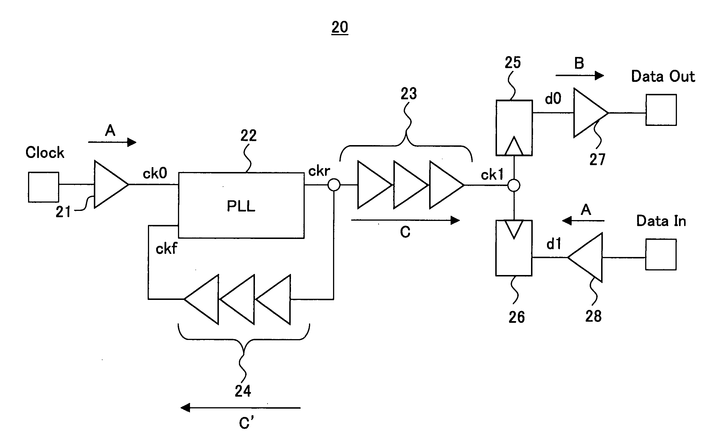
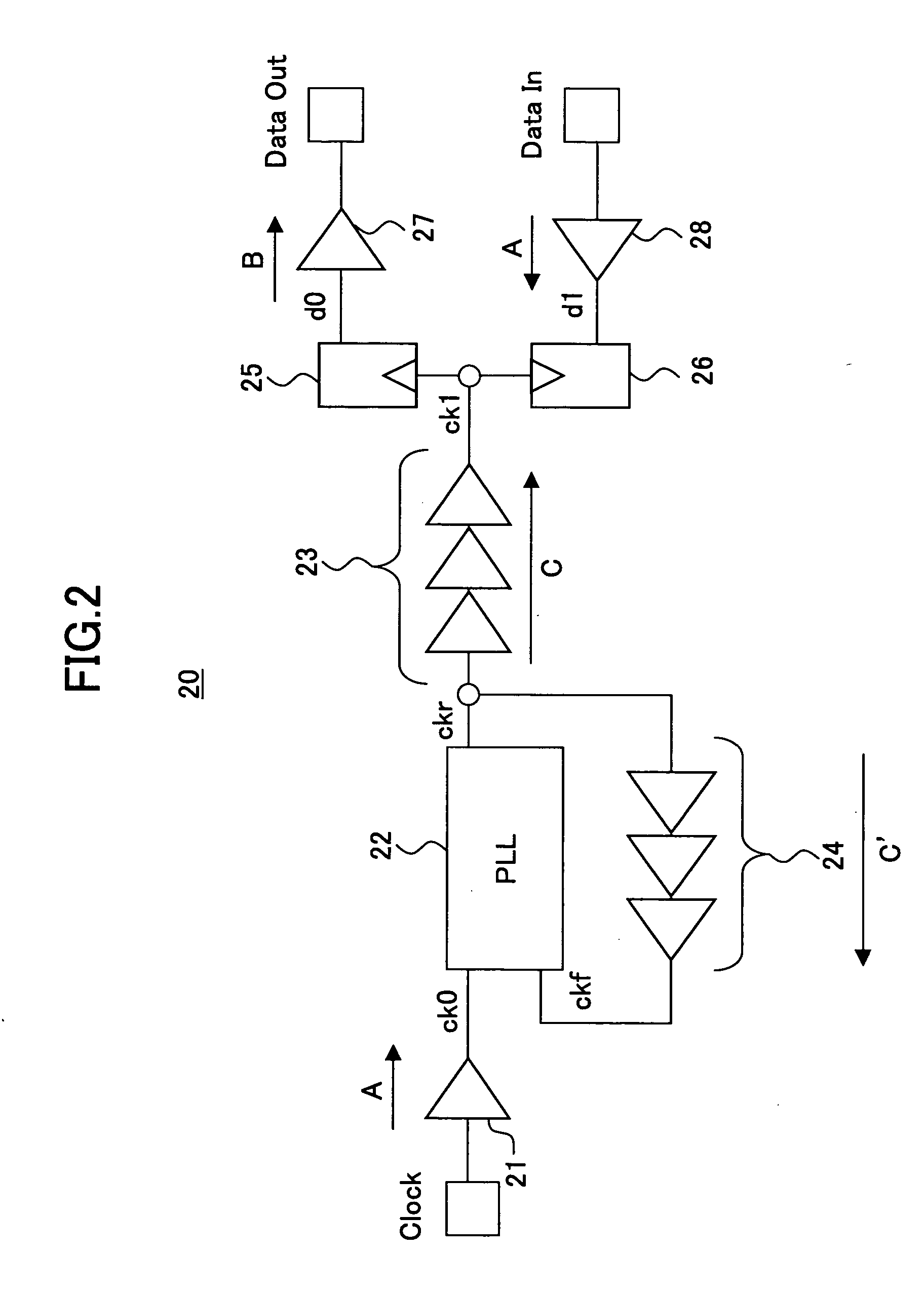
[0054]FIG. 6 is a circuit diagram showing an example of a timing adjustment circuit according to the present invention. A timing adjustment circuit 30 of FIG. 6 includes a clock input circuit 31, a PLL circuit 32, a clock tree 33, a feedback tree 34, an output-purpose flip-flop (output data circuit) 35, an input-purpose flip-flop (input data circuit) 36, a data output circuit 37, a data input circuit 38, a dummy input / output circuit (first timing correction circuit) 39, and an input timing correction circuit (second timing correction circuit) 40.

[0055] The clock input circuit 31 receives a clock signal Clock supplied from the exterior of the chip, and supplies the received signal to the PLL circuit 32 as an input clock signal ck0. The clock input circuit 31 has an inherent delay time A. The input clock signal ck0 has a delay equal to the delay time A relative...


PUM


Abstract

A circuit for timing adjustment includes a PLL circuit configured to generate a phase-adjusted clock signal in response to phase comparison between an input clock signal and a delayed clock signal, a feedback path configured to delay the phase-adjusted clock signal for provision as the delayed clock signal to the PLL circuit, a first timing correction circuit configured to add a predetermined delay time to the feedback path, an output data circuit configured to supply output data at first timing responsive to the phase-adjusted clock signal, a second timing correction circuit configured to delay the first timing by the predetermined delay time to generate second timing different from the first timing, and an input data circuit configured to latch input data at the second timing.

Description

CROSS-REFERENCE TO RELATED APPLICATIONS [0001] The present application is based upon and claims the benefit of priority from the prior Japanese Patent Applications No. 2004-136248 filed on Apr. 30, 2004 and No. 2004-296469 filed on Oct. 8, 2004, with the Japanese Patent Office, the entire contents of which are incorporated herein by reference. BACKGROUND OF THE INVENTION [0002] 1. Field of the Invention [0003] The present invention generally relates to timing adjustment circuits used in clock synchronous apparatuses, and particularly relates to a timing adjustment circuit for adjusting the timing of clock synchronization of a data input / output interface. [0004] 2. Description of the Related Art [0005]FIG. 1 is an illustrative drawing showing an example of a construction in which semiconductor chips of the clock synchronous type are connected to each other. Chips 10 through 13 shown in FIG. 1 operate in synchronization with a clock signal. A data signal output from the chip 10 in syn...

Claims


Application Information

Patent Timeline
IPC IPC(8): G06F13/16H03L7/06H03L7/08H03L7/081
CPCG06F13/1689H03L7/0812H03L7/08H03L7/0816
Inventor KAWASAKI, KENICHI
Owner FUJITSU LTD
Why Eureka
Try Eureka