Bake apparatus for use in spin-coating equipment

a technology of spin-coating equipment and baking apparatus, which is applied in the direction of steam generation using steam absorption, chemical vapor deposition coating, combustion air/fuel air treatment, etc., can solve the problems of unsatisfactory critical dimension (cd) of the pattern formed on the wafer, and the defect of the pattern formed

Inactive Publication Date: 2005-11-03
SAMSUNG ELECTRONICS CO LTD
View PDF8 Cites 11 Cited by
  • Summary
  • Abstract
  • Description
  • Claims
  • Application Information

AI Technical Summary

Problems solved by technology

This causes variations in the thickness of the layer of photoresist which, in turn, results in defects in the pattern formed using the pat

Method used


Image

  • Bake apparatus for use in spin-coating equipment
  • Bake apparatus for use in spin-coating equipment

Examples


Embodiment Construction

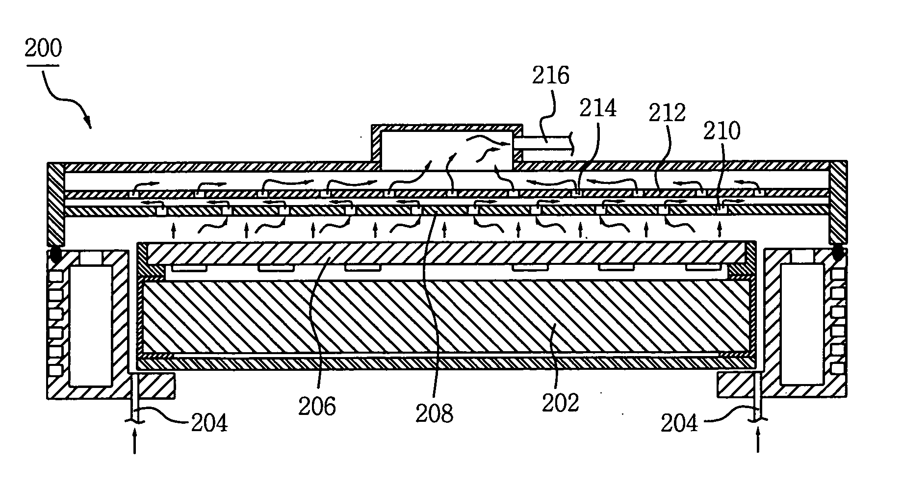
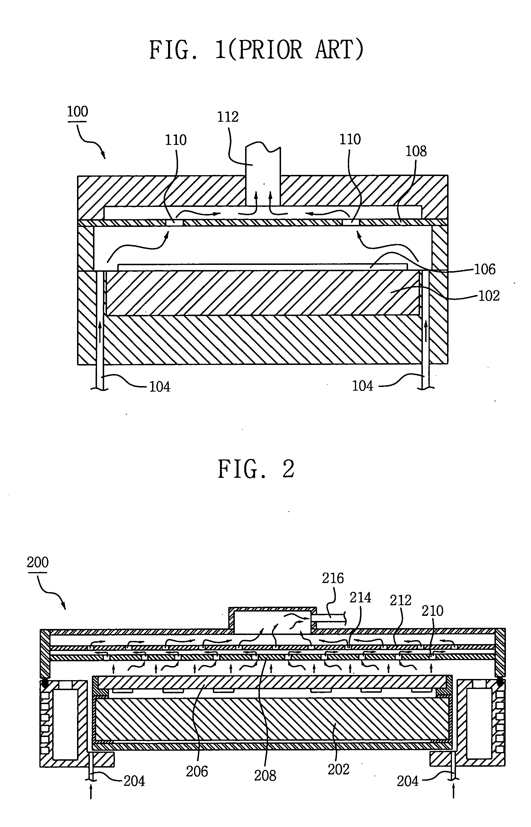
[0024] Bake apparatus for use in a spin-coater according to the present invention will be described in detail with reference to FIG. 2. For purposes of clarity, though, a detailed description of known functions and systems associated with bake apparatus in general has been omitted.

[0025] Referring to FIG. 2, the bake apparatus includes a cylindrical chamber 200, a hot plate 202 installed within the chamber 200, a first circular buffer plate 208 disposed within an upper part of the chamber 200, and a second circular buffer plate 212 disposed within the upper part of the chamber 200 at a predetermined distance above the first buffer plate 208. A wafer 206 is mounted on the hot plate 202, and the hot plate 202 heats the wafer 206 to predetermined temperature and thereby bakes a photoresist layer on the wafer 206.

[0026] In addition, the bake apparatus has an air injection passageway 204 for injecting a predetermined quantity of gas (air) into the chamber 200. The first buffer plate 20...


PUM


Abstract

Bake apparatus for use in baking a substrate, such as a semiconductor wafer, includes a chamber, a hot plate installed within the chamber, and first and second buffer plates for uniformly dispersing hot gas. The hot plate is configured to support the semiconductor wafer. The gas is injected into the chamber through an air passageway and is exhausted through an air exhaust opening. The first buffer plate is disposed within an upper part of the chamber so as to uniformly disperse the gas within the chamber. The second buffer plate is disposed above the first buffer plate. The first and second buffer plates each have a number of discharge holes by which the gas is uniformly discharged from the chamber to the exhaust opening.

Description

BACKGROUND OF THE INVENTION [0001] 1. Field of the Invention [0002] The present invention relates to the manufacturing of semiconductor devices and the like. More specifically, the present invention relates to bake apparatus for baking a substrate, such as a semiconductor wafer, coated with photoresist. [0003] 2. Description of the Related Art [0004] Semiconductor devices are generally manufactured by subjecting a substrate, e.g., a wafer, to ion implantation, deposition, diffusion, photolithography and etching processes. The aim of these processes, especially the photolithography process, is to form a desired pattern on the wafer. [0005] The photolithography process includes coating, exposing and developing processes. In the coating process, the photoresist is dispensed onto the wafer and the wafer is rotated at a high speed so that the wafer is covered with a layer of photoresist to a desired thickness. In the exposure process, the wafer covered with the photoresist and a correspo...

Claims


Application Information

Patent Timeline
IPC IPC(8): G03C5/00H01L21/324G03F7/16H01L21/00
CPCG03F7/162H01L21/67109G03F7/168H01L21/324
Inventor LEE, MYOUNG-KUY
Owner SAMSUNG ELECTRONICS CO LTD
Why Eureka
Try Eureka