

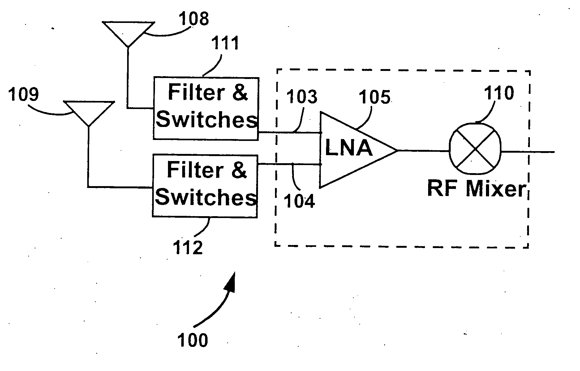
Dual-band CMOS front-end with two gain modes
a cmos front-end and gain mode technology, applied in the direction of gated amplifiers, low-noise amplifiers, transportation and packaging, etc., can solve the problems of increasing the number of chip components, the overall die size, and the die cost is significantly increased, so as to improve the effect of reducing the footprint of the rf receiver
- Summary
- Abstract
- Description
- Claims
- Application Information
AI Technical Summary
Benefits of technology
Problems solved by technology
Method used
Image

Examples
examples
[0047] The present invention is further illustrated by the following specific examples, which should not be constructed as limiting the scope or content of the invention in any way. Winderman, “Perform True DSB-To-SSB Noise-Figure Conversions,” Microwaves, pp. 69, July 1980, the single-side band (SSB) NF is estimated to be 2.6 dB, which is considered excellent.
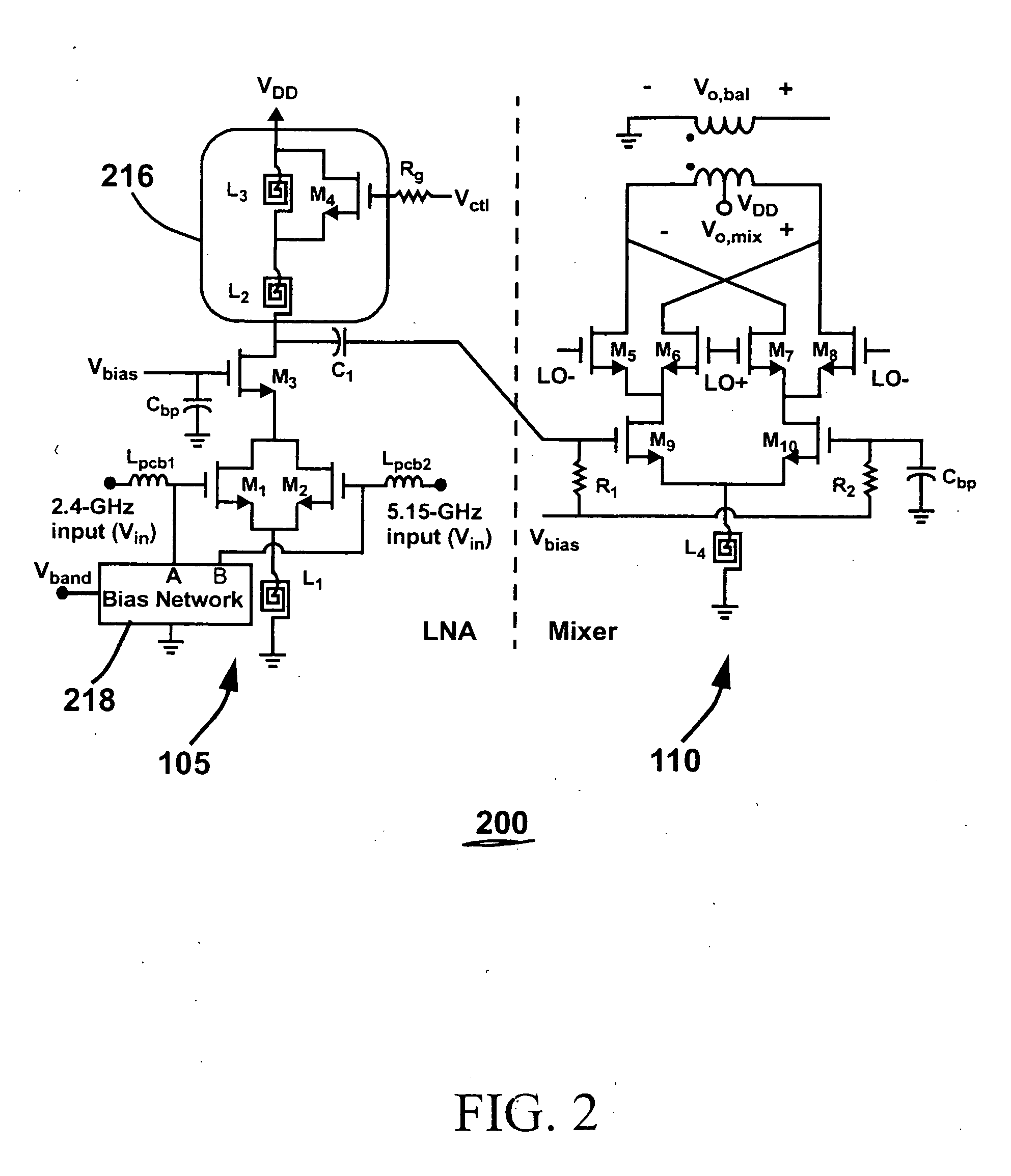
[0048] The 2.4 GHz band measurements shown in FIG. 5(a) demonstrates that the LNA output is well tuned at the high gain mode. However, the 5.15-GHz band measurements in FIG. 7(b) shows that the LNA output is mis-tuned at the high gain mode since the gain is peaked at a frequency of about 4.5 GHz. However, because of moderate tank Q, even with the resonant frequency lower than the design value, 17 dB power gain is still obtained at 5.15 GHz by increasing the LNA bias current to 9 mA. Changing the bias current from 3 mA (used for 4.4 GHz operation) to 9 mA increased the power gain at 5.15 GHz by about 4 dB. The voltage gain of ...
PUM
 Abstract
Description
Claims
Application Information