Solid-state imaging device and driving method therefor

a technology of solid-state imaging and driving methods, which is applied in the direction of radioation control devices, television systems, and scanning details of television systems, can solve problems such as noise and shading, and achieve the effects of suppressing well potential fluctuations, and preventing noise and shading

Active Publication Date: 2005-11-10
SONY CORP
View PDF7 Cites 22 Cited by
  • Summary
  • Abstract
  • Description
  • Claims
  • Application Information

AI Technical Summary

Benefits of technology

[0007] The present invention has been made in view of the above circumstance. Accordingly, there is a need for providing a solid-state imaging device and driving method therefor that, by suppressing a fluctuation in well potential of a pixel array while a signal is being read from a pixel, prevent generation of noise and shading caused by the fluctuation in well potential.
[0011] According to an embodiment of the present invention, by suppressing a fluctuation in well potential in a pixel array, caused by a fluctuation in potential of a signal line, it is ensured that the fluctuation in well potential is prevented from affecting a reset level and a signal level. Therefore, this prevents generation of noise and shading caused by the fluctuation in well potential.

Problems solved by technology

The superimposed fluctuation causes noise and shading (broad unevenness on a captured image on the screen).

Method used


Image

  • Solid-state imaging device and driving method therefor
  • Solid-state imaging device and driving method therefor
  • Solid-state imaging device and driving method therefor

Examples


first embodiment

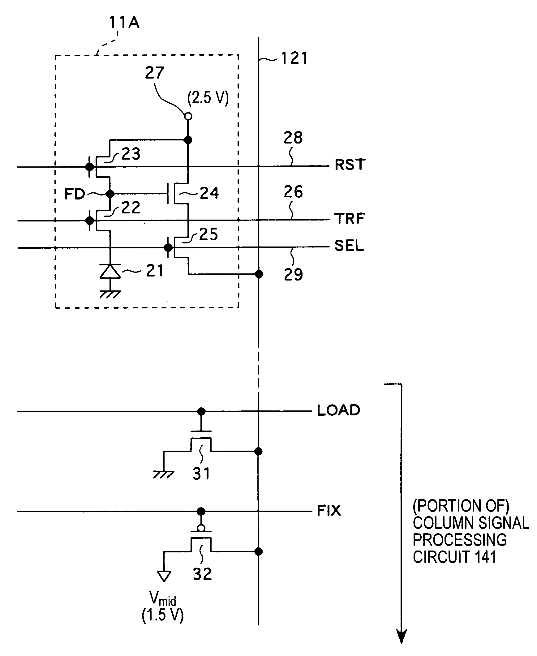
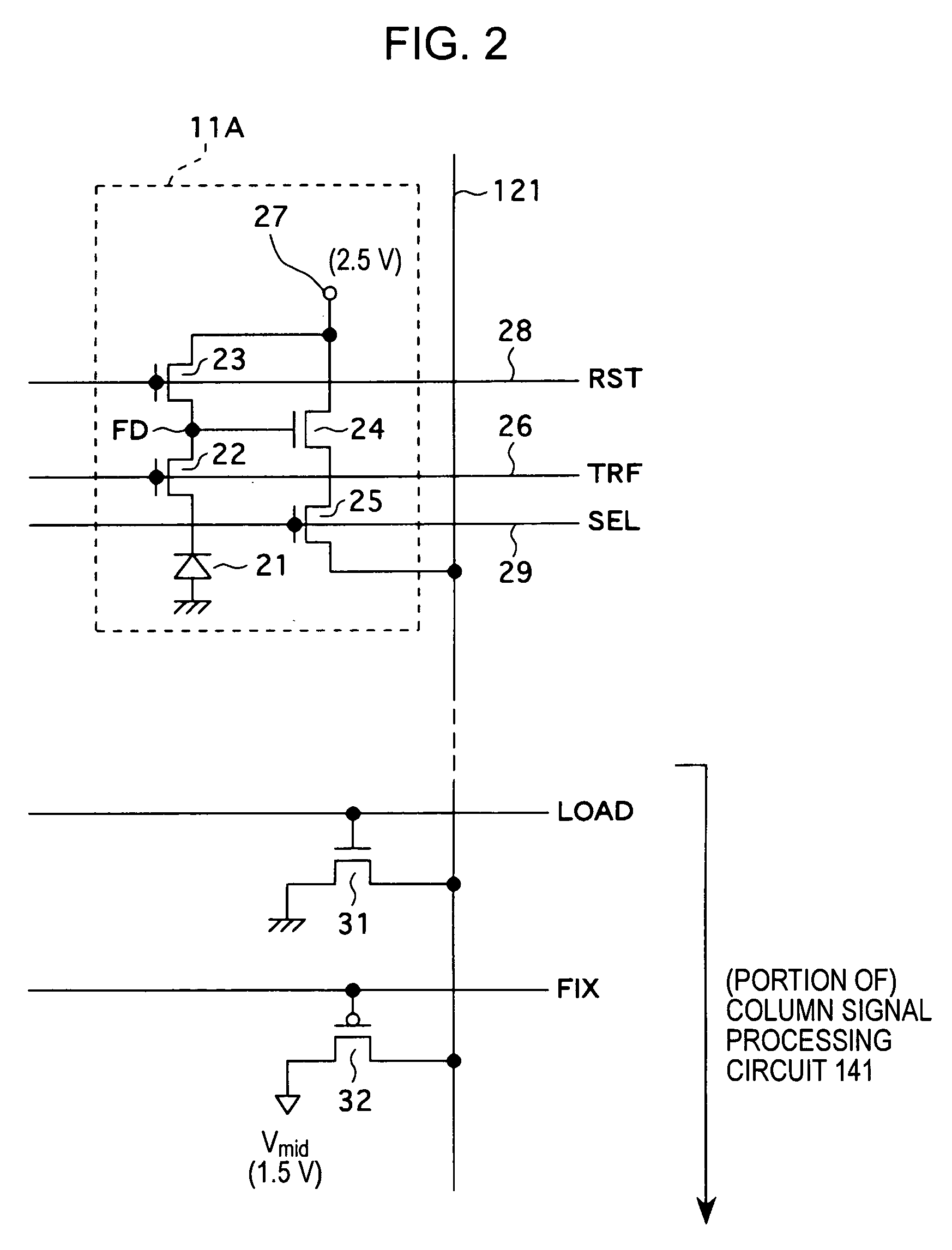
[0026]FIG. 2 is a circuit diagram showing a substantial part of a CMOS image sensor according to a first embodiment of the present invention. In other words, FIG. 2 shows portions of one pixel and the column signal processing circuit 141. Specifically, FIG. 2 is a circuit diagram only showing one of pixels 11A and the portion of one column signal processing circuit 141 connected to one vertical signal line 121 in the column to which the pixel 11A belongs.

[0027] As shown in FIG. 2, the pixel 11A includes a photoelectric conversion element, for example, a photodiode 21, and four transistors, that is, a transfer transistor 22, a reset transistor 23, an amplifying transistor 24, and a selecting transistor 25. FIG. 2 shows a case in which N-channel MOS transistors are used as the transfer transistor 22, the reset transistor 23, the amplifying transistor 24, and the selecting transistor 25. However, P-channel transistors may be used.

[0028] The photodiode 21 has an anode connected to hav...

second embodiment

[0047]FIG. 4 is a circuit diagram showing a substantial part of a CMOS image sensor according to a second embodiment of the present invention. In other words, FIG. 4 shows portions of a pixel and a column signal processing circuit. Specifically, FIG. 4 is a circuit diagram only showing one of pixels 11B and a portion of one column signal processing circuit 141 connected to one vertical signal line 121 in the column to which the pixel 11B belongs.

[0048] As shown in FIG. 4, the pixel 11B includes a photoelectric conversion element, for example, a photodiode 41, and three transistors, that is, a transfer transistor 42, a reset transistor 43, and an amplifying transistor 44. FIG. 4 shows a case in which N-channel MOS transistors are used as the transfer transistor 42, the reset transistor 43, and the amplifying transistor 44. Instead, P-channel MOS transistors may be used.

[0049] The photodiode 41 has an anode connected to the ground. The photodiode 41 converts incident light into sign...


PUM


Abstract

A solid-state imaging device includes a pixel array including pixels two-dimensionally arranged in matrix form, with a signal line provided in each column of the arranged pixels, each pixel including a photoelectric conversion element, and a fixing unit fixing the potential of the signal line, which is obtained before the pixel has an operating period, to an intermediate potential between a first power-supply potential and a second power-supply potential.

Description

CROSS REFERENCES TO RELATED APPLICATIONS [0001] The present invention contains subject matter related to Japanese Patent Application JP 2004-129388 filed in the Japanese Patent Office on Apr. 26, 2004, the entire contents of which are incorporated herein by reference. BACKGROUND OF THE INVENTION [0002] 1. Field of the Invention [0003] The present invention relates to solid-state imaging devices and driving methods therefor, and in particular, to a complementary metal-oxide semiconductor (CMOS) or metal-oxide semiconductor (MOS) solid-state imaging device and a driving method therefor. [0004] 2. Description of the Related Art [0005] CMOS solid-state imaging devices (hereinafter referred to as “CMOS image sensors”), which can be produced in a process similar to that for CMOS integrated circuits, are known as solid-state imaging devices (see, for example, Japanese Patent Specification No. 3000782). Regarding the CMOS image sensors, by using miniaturization technology related to a CMOS ...

Claims


Application Information

Patent Timeline
Patent Type & Authority Applications(United States)
IPC IPC(8): H01L27/146H04N25/00H04N25/65
CPCH04N5/3658H04N5/357H04N5/378H01L27/14612H01L27/14643H04N25/766H04N25/767H04N25/77H04N25/616H04N25/78H04N25/677H04N25/60H04N25/75H04N25/772H04N25/778
Inventor MABUCHI, KEIJIWAKANO, TOSHIFUMIKOSEKI, KEN
Owner SONY CORP
Why Eureka
Try Eureka