Semiconductor device and manufacturing method thereof

a technology of semiconductor devices and manufacturing methods, applied in the direction of semiconductor devices, basic electric elements, electrical appliances, etc., can solve the problems of short circuit between gates, achieve good and improve the embeddability of embedded insulating films

Inactive Publication Date: 2005-11-17
SONY CORP
View PDF6 Cites 10 Cited by
  • Summary
  • Abstract
  • Description
  • Claims
  • Application Information

AI Technical Summary

Benefits of technology

[0022] In this method, the underlying insulating film containing the silicon nitride film is first formed on the inner wall of the filling portion by the chemical vapor deposition method using the material gas containing hexachlorodisilane. This underlying insulating film produces a surface condition having good embeddability of the embedded...

Problems solved by technology

However, when the width of the trench 105 is as narrow as not more than 100 nm, the embeddability of the HDP-CVD may arise a problem that a void 110 occurs as shown in FIG. 11B, and the void 110 rem...

Method used


Image

  • Semiconductor device and manufacturing method thereof
  • Semiconductor device and manufacturing method thereof
  • Semiconductor device and manufacturing method thereof

Examples


first embodiment

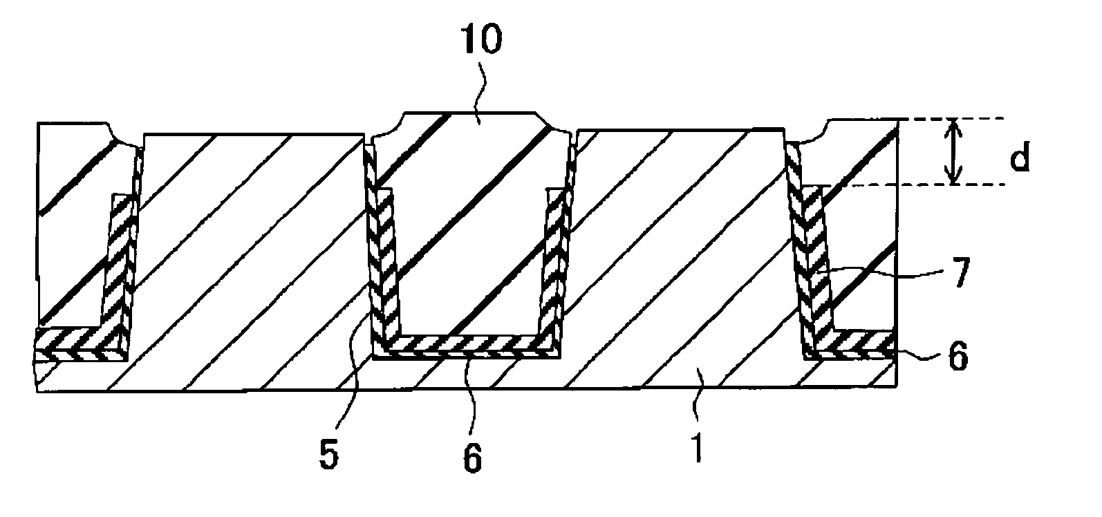
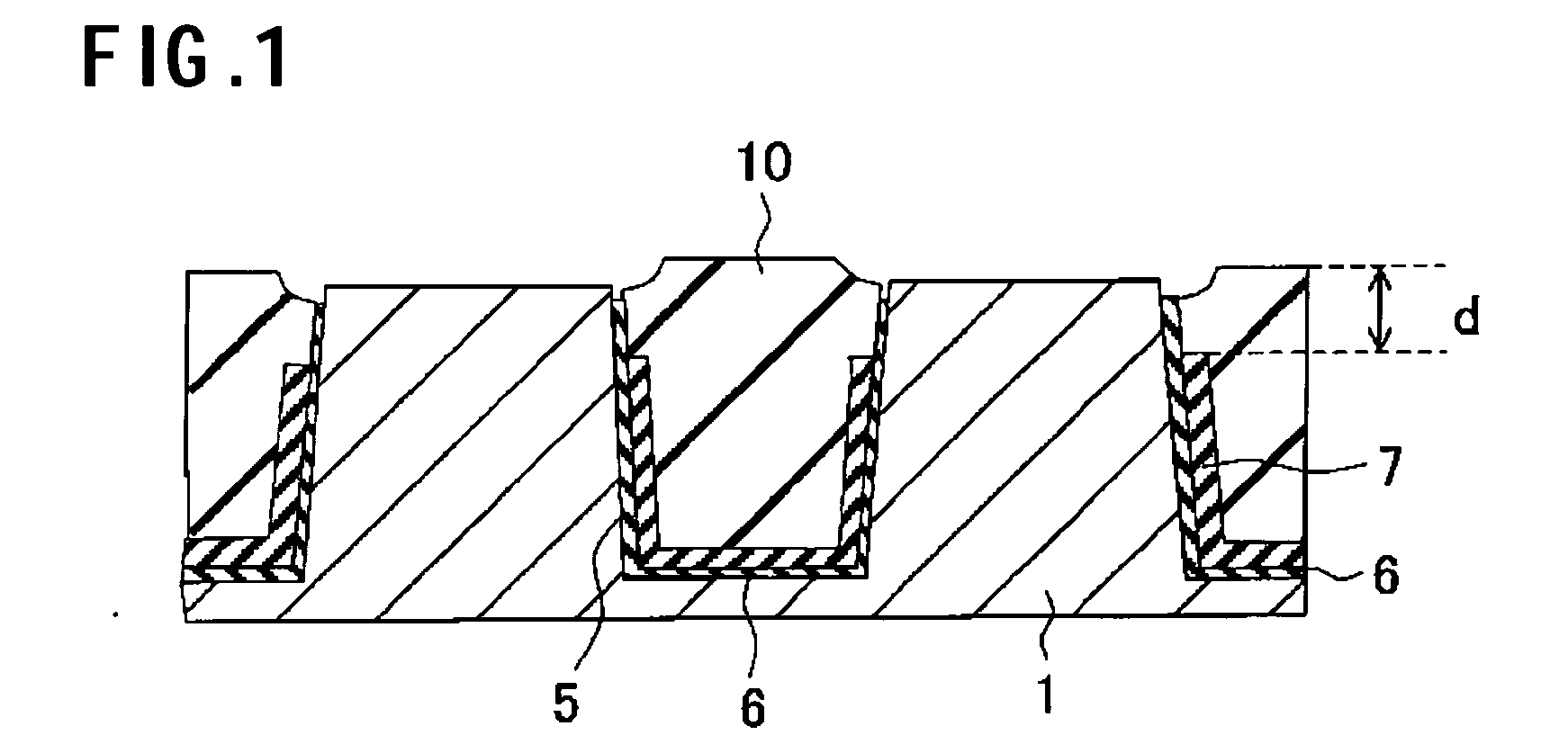
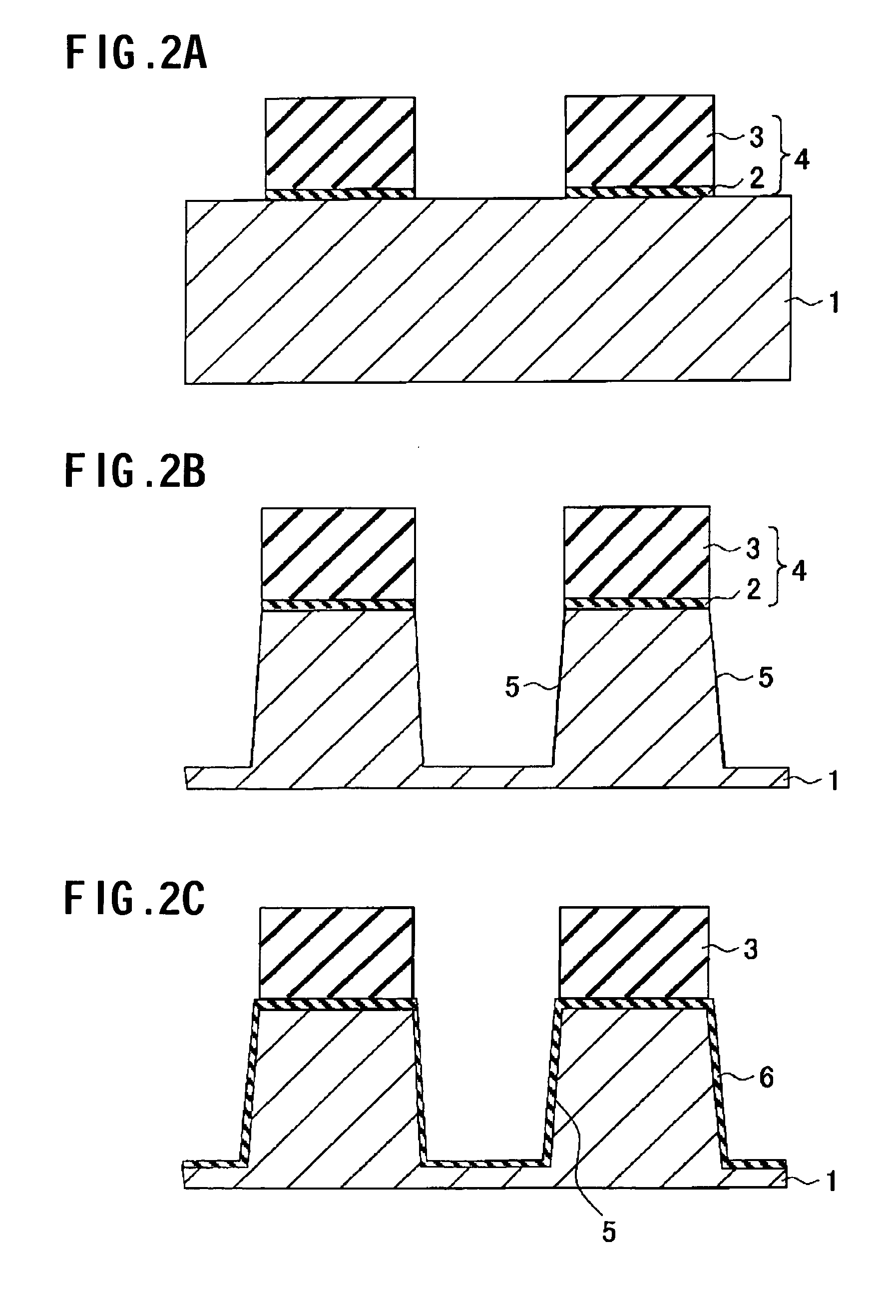
[0029]FIG. 1 is a sectional view showing a main part of an embedded structure in a semiconductor device according to a first preferred embodiment.

[0030] In the semiconductor device of FIG. 1, a trench (filling portion) 5 is formed at an element isolation region of a semiconductor substrate such as of silicon (hereinafter referred to simply as a substrate) 1. On the inner wall of the trench 5, a silicon thermal oxide film 6 is formed, and a silicon nitride film (underlying insulating film) 7 is also formed.

[0031] The silicon nitride film 7 is a silicon nitride film formed by the chemical vapor deposition method using material gas containing hexachlorodisilane (HCD) Si2Cl6 (hereinafter referred to as HCD-silicon nitride film). The HCD-silicon nitride film 7 is disposed for producing surface condition to accelerate the growth rate of a silicon oxide film to be embedded within the trench 5.

[0032] The film thickness of the HCD-silicon nitride film 7 is preferably in a range of 0.5 nm ...

second embodiment

[0055]FIG. 7 is a sectional view showing important parts of an embedded structure in a semiconductor device according to a second preferred embodiment. Similar components are indicated with the same reference numerals as in FIG. 1, and their descriptions are omitted herein.

[0056] In the semiconductor device shown in FIG. 7, a silicon thermal oxide film 6 is formed on the inner wall of a trench (filling portion) 5 formed in a substrate 1, and an HCD-silicon nitride film 7 is also formed as in the first preferred embodiment.

[0057] The film thickness of the HCD-silicon nitride film 7 is preferably in the range of 0.5 nm to 50 nm, for example, for the same reason as in the first preferred embodiment. The end portion of the HCD-silicon nitride film 7 is preferably apart from the surface of the substrate 1 by a distance d of not more than 100 nm, for the same reason as in the first preferred embodiment.

[0058] A first embedded insulating film 11 composed of a silicon oxide film is forme...


PUM


Abstract

In order to improve embeddability of an embedded insulating film to a filling portion to have a preferable embedded structure, the present invention provides a semiconductor device having an embedded structure in which an embedded insulating film is embedded in a filling portion formed in or on a substrate. The embedded structure includes an underlying insulating film containing a silicon nitride film formed on an inner wall of the filling portion by a chemical vapor deposition method using material gas containing hexachlorodisilane, and an embedded insulating film formed by filling in the filling portion via the underlying insulating film.

Description

CROSS REFERENCES TO RELATED APPLICATIONS [0001] The present document contains subject matter related to Japanese Patent Application JP 2004-141584 filed in the Japanese Patent Office on May 11, 2004, the entire contents of which being incorporated herein by reference. BACKGROUND OF THE INVENTION [0002] 1. Field of the Invention [0003] The present invention relates to a semiconductor device and a manufacturing method thereof, such as a semiconductor device having an embedded structure in which an embedded insulating film is embedded within a trench formed in a semiconductor substrate, and a manufacturing method thereof. [0004] 2. Description of Related Art [0005] As technique of electrically isolating elements formed on a semiconductor substrate, shallow trench isolation structure (hereinafter referred to as “STI structure”) is known, in which a trench is formed in a semiconductor substrate and an insulating film is filled therein. This is disclosed in, for example, Japanese Patent A...

Claims


Application Information

Patent Timeline
IPC IPC(8): H01L21/76H01L21/318H01L21/762
CPCH01L21/76227H01L21/76224H01L21/02211H01L21/02271
Inventor NAGAOKA, KOHJIRO
Owner SONY CORP
Why Eureka
Try Eureka